The Voltage Divider
Found 8 free book(s)
Chapter 6: Voltage Regulator - Ajlon Tech
www.ajlontech.comA feedback voltage obtained from voltage divider R 1 and R 2 is applied to the op-amp’s non-inverting input and compared to the Zener voltage to control the drive current to the transistor. The current through resistor R S is thus controlled to drop a voltage across R S so that the output voltage is maintained.

Lecture 19 - MIT
web.mit.eduVoltage divider at input: Voltage divider at output: Loaded voltage gain: v in=R vs Rin +Rs vout =RL Avovin Rout +RL vout vs = Rin Rin +RS Avo RL RL +Rout +-vin +-Avovin vout Rout +-Rin Rs vs +-RL unloaded circuit output loading input loading. 6.012 Spring 2007 Lecture 19 8 Small-signal voltage gain Avo: draw small-signal

Lecture 20 Bipolar Junction Transistors (BJT): Part 4 ...
alan.ece.gatech.edu•Warning: Just like when a diode voltage exceeds a certain value, the non-linear behavior of the diode leads to distortion of the current/voltage curves (see previous lecture), if the inputs/outputs exceed certain limits, the full Ebers -Moll model ... Applying a voltage divider: BE /v.
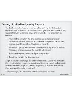
Solving circuits directly using Laplace
tuttle.merc.iastate.eduvoltage divider. = 1 sC R+ 1 sC +sL V i (s) V C (s) = Z C Z R +Z C +Z L V i (s) V C (s) = (1 1+sRC+s2LC)(V f s) = V f LC s(s2 +s R L + 1 LC) – + + – Z R V i (s) Z C V C (s) Z L Convert to the frequency domain. Z R = R

Data Sheet ADP172 - Analog Devices
www.analog.comApr 21, 2021 · Subtract the current from the external resistor divider network in the case of adjustable voltage output (as with the ADP172) from the ground current measured. 2 Based on an end-point calculation using 1 mA and 300 mA loads.

VOLTAGE TRANSFORMERS
www.gegridsolutions.comwatts at rated secondary voltage when rated phase-to-ground voltage is impressed across the capacitance voltage divider. The rated burden of the device is the sum of the watt burdens that may be impressed on both secondary windings simultaneously. Adjustment capacitors are provided in the device for connecting in parallel with the
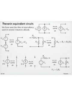
Thevenin equivalent circuits - Iowa State University
tuttle.merc.iastate.eduJun 10, 2014 · The open-circuit voltage / short-circuit current approach can be used to calculate the Thevenin equivalent for a known circuit. Consider the circuit from slide 4: + – V S R 1 R 2 I S 9V 6 mA 1.5 k! 3 k! Open-circuit voltage – Use whatever method you prefer. We’ll use node voltage in this case. + – V S R 1 R 2 I S v a + – v oc YRF= YD ...

Operational amplifier stability compensation methods for ...
www.st.comFigure 9. Voltage follower configuration Figure 10. Closed loop gain measured for a voltage follower configuration Voltage Follower Configuration - Closed Loop Gain-40-30-20-10 0 10 20 1.E+03 1.E+04 1.E+05 1.E+06 1.E+07 Frequency (Hz) Gain (dB) Gain without CL Gain with CL = 550 pF TS507 : Vcc = 5 V Vicm = 2,5 V T = 25 °C RL = 10 kΩ Without ...