Search results with tag "Pcb layout"

USB 3.0 Hub Controller
jfd-ic.comThe purpose of this document is to provide suggestions for the design of circuit and PCB layout regarding the USB 3.0 Hub Controllers of Genesys Logic Inc. 2. CIRCUIT DESIGN AND PCB LAYOUT GUIDELINES 2.1 AC Coupling Capacitors PHY is a component where the transmitter and receiver are located and operated together. The AC coupling
CHAPTER 12: PRINTED CIRCUIT BOARD (PCB) DESIGN ISSUES
www.analog.comBASIC LINEAR DESIGN 12.4 Figure 12.1: Analog and Digital Circuits Should Be Partitioned on PCB Layout The layout of the evaluation board is optimized in terms of grounding, decoupling, and signal routing and can be used as a model when laying out the ADC section of the PC

AN1258 - Op Amp Precision Design: PCB Layout Techniques
ww1.microchip.comOp Amp Precision Design: PCB Layout Techniques. AN1258 DS01258B-page 2 2009-2012 Microchip Technology Inc. The linearized relationship between temperature and thermoelectric voltage, for small temperature ranges, is given in Equation 1. The Seebeck coefficients for the

BGM220S Wireless Gecko Bluetooth Module Data Sheet
www.silabs.comParameter With optimal layout Note Efficiency -1.4 to -2.6 dB Antenna efficiency, gain and radiation pattern are highly depend-ent on the application PCB layout and mechanical design. Refer to 7. Design Guidelines for recommendations to achieve optimal antenna performance. Peak gain 1.5 dBi Table 3.2. Antenna Efficiency and Peak Gain (BGM220S22A)

A Hardware Designer's Informal Guide to Xilinx® Zynq ...
fidus.comApr 06, 2020 · acceptable, etc). This is a good time to have a discussion with your PCB layout designer. Having a great understanding of all these elements will allow you to identify the family member to target. Warning! Cost drives all. I intentionally left cost out of this discussion because it can’t be described or quantified in any more
NexFETTM High Performance MOSFETs - Texas Instruments
www.ti.comA number of methods have been widely used to minimize the switch node ringing. These methods are listed as follows: 1. Careful PCB layout to minimize the parasitic loop inductance in circuit [1].
UNDERSTANDING AND CONTROLLING COMMON-MODE …
www.hottconsultants.com©Henry W. Ott HOC ELECTROMAGNETIC COMPATIBILITY COMMON-MODE & DIFFERENTIAL MODE NOISE! Differential-Mode Noise — Involves the Normal Operation of the Circuit — Currents Flowing Around Loops — Is Documented • Schematics • PCB Layout • Wiring Diagrams — Is Easy to Understand Common-Mode Noise
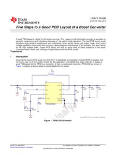
Five Steps to a Good PCB Layout of the Boost Converter
www.ti.comIMPORTANT NOTICE FOR TI DESIGN INFORMATION AND RESOURCES Texas Instruments Incorporated (‘TI”) technical, application or other design advice, …