Search results with tag "Vref"
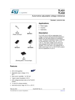
TL431 TL432 - STMicroelectronics
www.st.comV ref Reference input voltage VKA = V , Ik = 10mA Tmin Tamb Tmax 2.44 2.41 2.495-2.55 2.58 2.47 2.44 2.495-2.52 2.55 V Vref Reference input voltage deviation overtemperature range(1) VKA = Vref, Ik = 10mA, Tmin Tamb Tmax - 730- 730mV Ratio of change in reference input voltage to change
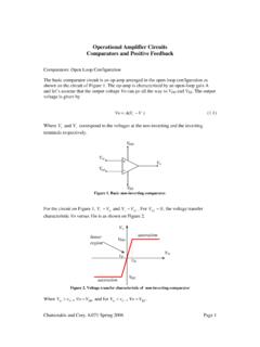
Operational Amplifier Circuits Comparators and Positive ...
ocw.mit.eduWhere V+ and V− correspond to the voltages at the non-inverting and the inverting terminals respectively. VDD V V in V o V EE ref Figure 1. Basic non-inverting comparator. For the circuit on Figure 1, V+ =Vin and V− = Vref . For Vref = 0 , the voltage transfer characteristic Vo versus Vin is as shown on Figure 2. V o V in V EE V DD v δ+ v ...
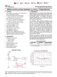
Low-Drift, Low-Power, Dual-Output, VREF and …
www.ti.comina213 v in ref2030 v ref 3.0 v v bias 1.5 v en adc gnd load r shunt isense v in- v in+ ref v out power supply-0.05 -0.04 -0.03 -0.02 -0.01 0 0.01 0.02 0.03 0.04 0.05 ± 75 ± 50 ± 25 0 25 50 75 100 125 150

624BLD RevF MULTI - FAAC
www.faac.co.uk3 1. WARNINGS Attention: Before attempting any work on the control unit (connections, maintenance), always turn off power. - Install, upstream of the system, a differential thermal breaker with adequate tripping threshold.