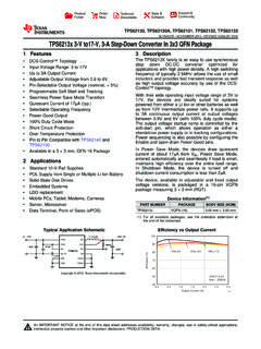
Transcription of 10 A microBUCK SiC402A/B Integrated Buck …
1 sic402a , Siliconix S14-2048-Rev. C, 13-Oct-141 Document Number: 63729 For technical questions, contact: DOCUMENT IS SUBJECT TO CHANGE WITHOUT NOTICE. THE PRODUCTS DESCRIBED HEREIN AND THIS DOCUMENTARE SUBJECT TO SPECIFIC DISCLAIMERS, SET FORTH AT A microBUCK sic402a /BIntegrated buck Regulator with Programmable LDODESCRIPTIONThe vishay Siliconix SiC402A/B an advanced stand-alone synchronous buck regulator featuring Integrated power MOSFETs, bootstrap switch, and a programmable LDO in a space-saving PowerPAK MLP55-32L pin SiC402A/B are capable of operating with all ceramic solutions and switching frequencies up to 1 MHz.
2 The programmable frequency, synchronous operation and selectable power-save allow operation at high efficiency across the full range of load current. The internal LDO may be used to supply 5 V for the gate drive circuits or it may be bypassed with an external 5 V for optimum efficiency and used to drive external n-channel MOSFETs or other loads. Additional features include cycle-by-cycle current limit, voltage soft-start, under-voltage protection, programmable over-current protection, soft shutdown and selectable power-save. The vishay Siliconix SiC402A/B also provides an enable input and a power good See High Output Voltage Operation sectionFEATURES High efficiency > 95 % 10 A continuous output current capability Integrated bootstrap switch Programmable 200 mA LDO with bypass logic Temperature compensated current limit All ceramic solution enabled Pseudo fixed-frequency adaptive on-time control Programmable input UVLO threshold Independent enable pin for switcher and LDO Selectable ultra-sonic power-save mode ( sic402a ) Selectable power-save mode (SiC402B)
3 Programmable soft-start and soft-shutdown 1 % internal reference voltage Power good output Over-voltage and under-voltage protections PowerCAD simulation software available at Material categorization: for definitions of compliance please see APPLICATIONS Notebook, desktop, and server computers Digital HDTV and digital consumer applications Networking and telecommunication equipment Printers, DSL, and STB applications Embedded applications Point of load power suppliesTYPICAL APPLICATION CIRCUIT AND PACKAGE OPTIONST ypical Application Circuit for SiC402A/B (PowerPAK MLP55-32L)
4 PRODUCT SUMMARYI nput Voltage Range3 V to 28 VOutput Voltage V to VIN x a Operating Frequency200 kHz to 1 MHzContinuous Output Current10 APeak Efficiency95 %PackagePowerPAK MLP55-32 LPAD 1 AGNDLXPAD 3 LXPAD 2 VINPGNDLXPGNDPGNDPGNDPGNDPGND1718192021 TONAGNDEN\ VEN/PSV (Tri-State)LDO_ENPGND3130 292526272832 sic402a , Siliconix S14-2048-Rev. C, 13-Oct-142 Document Number: 63729 For technical questions, contact: DOCUMENT IS SUBJECT TO CHANGE WITHOUT NOTICE. THE PRODUCTS DESCRIBED HEREIN AND THIS DOCUMENTARE SUBJECT TO SPECIFIC DISCLAIMERS, SET FORTH AT CONFIGURATION (Top View) SiC402A/B Pin Configuration (Top View)PIN DESCRIPTIONPIN NUMBERSYMBOL DESCRIPTION1 FBFeedback input for switching regulator used to program the output voltage - connect to an external resistor divider from VOUT to output voltage sense pin - also the input to the internal switch-over between VOUT and VLDO.
5 The voltage at this pin must be less than or equal to the voltage at the VDD supply for the IC - when using the internal LDO as a bias power supply, VDD is the LDO output. When using an external power supply as the bias for the IC, the LDO output should be , 30, PAD 1 AGNDA nalog ground5 FBLF eedback input for the internal LDO - used to program the LDO output. Connect to an external resistor divider from VDD to , 9 to 11, PAD 2 VINI nput supply voltage7 SSThe soft start ramp will be programmed by an internal current source charging a capacitor on this pin - connect a capacitor of at least 100 nF from BST to LX to develop the floating supply for the high-side gate , 14 NCNo connection13 LXBSTLX Boost - connect to the BST to 25, PAD 3 LXSwitching (phase) node15 to 22 PGNDP ower ground26 PGOODOpen-drain power good indicator - high impedance indicates power is good.
6 An external pull-up resistor is limit sense pin - used to program the current limit by connecting a resistor from ILIM to sense - connects to RILIM29EN/PSVE nable/power-save input for the switching regulator - connect to AGND to disable the switching regulator, connect to VDD to operate with power-save mode and float to operate in forced continuous programming input - set the on-time by connecting through a resistor to input for the LDO - connect ENL to AGND to disable the LDO. Drive with logic signal for logic control, or program the VIN UVLO with a resistor divider between VIN, ENL, and 1 AGNDLXPAD 3 LXPAD 2 VINPGNDLXPGNDPGNDPGNDPGNDPGND1718192021t ONAGNDEN\PSVLXILIMPGOODBSTVINFBLAGNDVDDV OUTFB12345768 SSPGNDVINVINVINNCLXNC910111213141516 PGND24LX2322 ENL31 30 292526272832 ORDERING INFORMATIONPART NUMBERPACKAGEMARKING(LINE 1: P/N)SiC402 ACD-T1-GE3 PowerPAKMLP55-32 LSiC402 ASiC402 BCD-T1-GE3 SiC402 BSiC402 DBReference BoardFormat: Line 1: Dot Line 2: P/N Line 3: Siliconix Logo + LOT Code + ESD Symbol Line 4.
7 Factory Code + Year Code + Work Week CodeP/NFywwIISiC402A, Siliconix S14-2048-Rev. C, 13-Oct-143 Document Number: 63729 For technical questions, contact: DOCUMENT IS SUBJECT TO CHANGE WITHOUT NOTICE. THE PRODUCTS DESCRIBED HEREIN AND THIS DOCUMENTARE SUBJECT TO SPECIFIC DISCLAIMERS, SET FORTH AT BLOCK DIAGRAMSiC402A/B Functional Block Diagram Stresses beyond those listed under Absolute Maximum Ratings may cause permanent damage to the device. These are stress ratings only, and functional operation of the device at these or any other conditions beyond those indicated in the operational sections of the specifications is not implied.
8 Exposure to absolute maximum rating/conditions for extended periods may affect device MAXIMUM RATINGS (TA = 25 C, unless otherwise noted)ELECTRICAL PARAMETER CONDITIONSLIMITSUNIT VINto to +30 VVINto to +30LX (transient < 100 ns)to PGND-2 to +30 VDDto to +6EN/PSV, PGOOD, ILIM, SS, VOUT, FB, FBLR eference to to +(VDD + )tONto to +(VDD - )BSTto to +6to to + to VINAGND to to + Junction Temperature150 CStorage Temperature-65 to 150 Power DissipationJunction to Ambient Thermal Impedance (RthJA) bIC section50 C/WMaximum Power DissipationAmbient temperature = 25 temperature = 100 ProtectionHBM2kVCDM1 NCNCSiC402A, Siliconix S14-2048-Rev.
9 C, 13-Oct-144 Document Number: 63729 For technical questions, contact: DOCUMENT IS SUBJECT TO CHANGE WITHOUT NOTICE. THE PRODUCTS DESCRIBED HEREIN AND THIS DOCUMENTARE SUBJECT TO SPECIFIC DISCLAIMERS, SET FORTH AT OPERATING RANGE (all voltages referenced to GND = 0 V)PARAMETER VIN3-28 VVDD to x Junction Temperature-40 to 125 CRecommended Ambient Temperature-40 to 85 ELECTRICAL SPECIFICATIONSPARAMETER SYMBOL TEST CONDITIONS UNLESS SPECIFIED VIN = 12 V, TA = +25 C for typ.
10 , -40 C to +85 C for min. and max., TJ = < 125 C, VDD = +5 V,typical application circuitLIMITS UNIT SuppliesInput Supply UVLO Threshold aVUVLOS ensed at ENL pin, at ENL pin, UVLO HysteresisVUVLO, UVLO ThresholdVUVLOM easured at VDD pin, at VDD pin, UVLO HysteresisVUVLO, Supply CurrentIINEN/PSV, ENL = 0 V, VIN = 28 V-1020 AStandby mode: ENL = VDD, EN/PSV = 0 V-160-VDD Supply CurrentIDDEN/PSV, ENL = 0 V-190300 sic402a , EN/PSV = V5V, no load(fSW = 25 kHz), VFB > V , EN/PSV = V5V, no loadVFB > V = 5 V, fSW = 250 kHz,EN/PSV = floating, no load b-8-VDD = 3 V, fSW = 250 kHz,EN/PSV = floating, no load b-5-FB On-Time ThresholdStatic VIN and RangefswContinuous mode operation-1000kHzMinimum fSW, ( sic402a only)