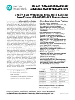
Transcription of ±10kV ESD-Protected, Quad 5V RS-485/RS-422 Transmitters
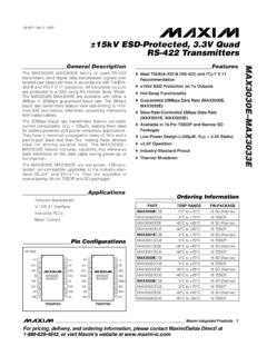
1 General DescriptionThe MAX3040 MAX3045 is a family of 5V quad RS-485/RS-422 Transmitters designed for digital data trans-mission over twisted-pair balanced lines. All transmitteroutputs are protected to 10kV using the Human BodyModel. In addition the MAX3040 MAX3045 withstand 4kV per IEC 1000-4-4 Electrical Fast Transient/BurstStressing. The MAX3040/MAX3043 (250kbps) and theMAX3041/MAX3044 ( ) are slew-rate limitedtransmitters that minimize EMI and reduce reflectionscaused by improperly terminated cables, thus allowingerror-free MAX3040 MAX3045 feature a hot-swap capabilitythat eliminates false transitions on the data cable duringpower-up or hot insertion. The MAX3042B/MAX3045 Bare optimized for data transfer rates up to 20 Mbps, theMAX3041/MAX3044 for data rates up to , andthe MAX3040/MAX3043 for data rates up to MAX3040 MAX3045 offer optimum performancewhen used with the MAX3093E or MAX3095 5V quaddifferential line receivers or MAX3094E/MAX3096 3 Vquad differential line receivers.
2 The MAX3040 MAX3045 are ESD-protected pin-compat-ible, low-power upgrades to the industry-standard SN75174 and DS26LS31C. They are available in space-saving TSSOP, narrow SO, and wide SO EquipmentIndustrial Motor ControlTransmitter for ESD-Sensitive ApplicationsHand-Held EquipmentIndustrial PLCsNetworkingFeatures ESD Protection: 10kV Human Body Model Single +5V Operation Guaranteed Device-to-Device Skew(MAX3040/MAX3041/MAX3043/MAX3044) Pin-Compatible with SN75174, 26LS31C andLTC487 Hot-Swappable for Telecom Applications Up to 20 Mbps Data Rate (MAX3042B/MAX3045B) Slew-Rate Limited (Data Rates at and250kbps) 2nA Low-Power Shutdown Mode 1mA Operating Supply Current 4kV EFT Fast Transient Burst Immunity per IEC1000-4-4 Level 2 Surge Immunity per IEC 1000-4-5,Unshielded Cable Model Ultra-Small 16-Pin TSSOP, 16-Pin Narrow SO, andWide 16-Pin SOMAX3040 MAX3045 10kV ESD-Protected, Quad 5V RS-485/RS-422 Transmitters_____Maxim Integrated Products1 Pin ConfigurationsSelector GuideOrdering Information19-2143; Rev 1.
3 12/01 Ordering Information continued at end of data pricing, delivery, and ordering information, please contact Maxim/Dallas Direct! at 1-888-629-4642, or visit Maxim s website at RANGEPIN-PACKAGEDATARATEMAX3040 CUE0 C to +70 C16 TSSOP250kbpsMAX3040 CSE0 C to +70 C16 Narrow SO250kbpsMAX3040 CWE0 C to +70 C16 Wide SO250kbpsMAX3040 EUE-40 C to +85 C16 TSSOP250kbpsMAX3040 ESE-40 C to +85 C16 Narrow SO250kbpsMAX3040 EWE-40 C to +85 C16 Wide SO250kbps16151413121110912345678T1 INVCCT4 INY4Z4EN34Z3Y3T3 INTOP VIEWMAX3040 MAX3041 MAX3042B16 TSSOP/SOY1Z1Y2EN12Z2T2 INGNDPARTDATA RATE(bps)INDUSTRY STANDARDPINOUTMAX3040250k75174, 34C87, , 34C87, LTC487 MAX3042B20M75174, 34C87, Configurations continued at end of data MAX3045 10kV ESD-Protected, Quad 5V RS-485/RS-422 Transmitters2_____ABSOLUTE MAXIMUM RATINGSELECTRICAL CHARACTERISTICS(VCC= +5V 5%, TA= TMINto TMAX, unless otherwise noted.)
4 Typical values are at VCC= +5V and TA= +25 C.) (Note 1)Stresses beyond those listed under Absolute Maximum Ratings may cause permanent damage to the device. These are stress ratings only, and functionaloperation of the device at these or any other conditions beyond those indicated in the operational sections of the specifications is not implied. Exposure toabsolute maximum rating conditions for extended periods may affect device voltages referenced to ground (GND).Supply Voltage (VCC)..+7 VControl Input Voltage (EN, EN, EN_) .. to (VCC+ )Driver Input Voltage (T_IN).. to (VCC+ )Driver Output Voltage (Y_, Z_)(Driver Disabled) .. to + Output Voltage (Y_, Z_)(Driver Enabled) .. to +10 VContinuous Power Dissipation (TA= +70 C)16-Pin TSSOP (derate C above +70 C) ..755mW16-Pin Narrow SO (derate C above +70 C).
5 696mW16-Pin Wide SO (derate C above +70 C) ..762mWOperating Temperature RangeMAX304_C_E ..0 C to +70 CMAX304_E_E ..-40 C to +85 CMaximum Junction Temperature ..+150 CStorage Temperature Range ..-65 C to +150 CLead Temperature (soldering, 10s) ..+300 CPARAMETERSYMBOLCONDITIONSMINTYPMAXUNITS DRIVERF igure 1, R = 50 Differential OutputVODF igure 1, R = 27 in Magnitude ofDifferential Output Voltage VODF igure 1, R = 50 or 27 (Note 2) Common-Mode OutputVoltageVOCF igure 1, R = 50 or 27 VCC / 23 VChange In Magnitude ofCommon-Mode Voltage VOCF igure 1, R = 50 or 27 (Note 2) High VoltageVIHT_IN, EN_, EN, Low VoltageVILT_IN, EN_, EN, Driver Input CurrentIHOTSWAPEN_, EN, EN (Note 3) 200 ADriver Input CurrentIINT_IN, EN_, EN, EN 1 ADriver Short-Circuit OutputCurrentISC-7V < VOUT < +10V (Note 4) 25 250mAMAX3040/MAX3041/MAX3042 BEN_ = GNDO utput Leakage (Y_, Z_)when DisabledMAX3043/MAX3044/MAX3045 BEN = GND, EN = VCC 1 AESD Protection (Y_, Z_)
6 Human Body Model 10kVElectrical Fast Transient/BurstImmunityIEC 1000-4-4 4kVSUPPLY CURRENTS upply CurrentICCNo load12mAMAX3040/MAX3041/MAX3042 BEN_ = GND, TA = +25 CSupply Current in ShutdownModeISHDNMAX3043/MAX3044/MAX3045 BEN = GND, EN = VCC, TA = +25 AMAX3040 MAX3045 10kV ESD-Protected, Quad 5V RS-485/RS-422 Transmitters_____ 3 SWITCHING CHARACTERISTICS MAX3040/MAX3043(VCC= +5V 5%, TA= TMINto TMAX, unless otherwise noted. Typical values are at VCC= +5V and TA= +25 C.)PARAMETERSYMBOLCONDITIONSMINTYPMAXUNI TSM aximum Data Propagation DelaytPHLF igures 2 and 3,RDIFF = 54 , CDIFF = Differential OutputRise-Time/Fall-TimetRFigures 2 and 3,RDIFF = 54 , CDIFF = stDSKEWD ifferent chips 350 Skew Driver to DrivertSSKEWSame chipFigures 2 and 3,RDIFF = 54 ,CDIFF = 50pF 100nsDriver Differential Output Skew| tPLH - tPHL |tSKEWF igures 2 and 3,RDIFF = 54 , CDIFF = 50pF 100nsDriver Enable to Output HightZHMAX3040, Figures 4 and 5, S2 closed,RL = 500 , CL= sDriver Enable from Shutdown toOutput HightZH(SHDN)Figures 4 and 5, S2 closed,RL = 500 , CL = sDriver Enable to Output LowtZLMAX3040, Figures 4 and 5, S1 closed,RL = 500 , CL = sDriver Enable from Shutdown toOutput LowtZL(SHDN)
7 Figures 4 and 5, S1 closed,RL = 500 , CL = sDriver Disable Time from LowtLZFigures 4 and 5, S1 closed,RL = 500 , CL = 15pF500nsDriver Disable Time from HightHZFigures 4 and 5, S2 closed,RL= 500 , CL = 15pF500nsSWITCHING CHARACTERISTICS MAX3041/MAX3044(VCC= +5V 5%, TA= TMINto TMAX, unless otherwise noted. Typical values are at VCC= +5V and TA= +25 C.)PARAMETERSYMBOLCONDITIONSMINTYPMAXUNI TSM aximum Data Propagation DelaytPHLF igures 2 and 3,RDIFF = 54 , CDIFF = 50pF70150nstF3370133 Driver Differential OutputRise-Time/Fall-TimetRFigures 2 and 3,RDIFF = 54 , CDIFF = 50pF3370133nstDSKEWD ifferent chips 52 Skew Driver to DrivertSSKEWSame chipFigures 2 and 3,RDIFF = 54 ,CDIFF = 50pF 15nsDriver Differential Output Skew| tPLH - tPHL |tSKEWF igures 2 and 3,RDIFF = 54 , CDIFF = 50pF 15nsDriver Enable to Output HightZHMAX3041, Figures 4 and 5, S2 closed,RL = 500 , CL = 100pF400nsMAX3040 MAX3045 10kV ESD-Protected, Quad 5V RS-485/RS-422 Transmitters4_____Note 1:All currents into the device are positive; all currents out of the device are negative.
8 All voltages are referenced to deviceground unless otherwise 2: VODand VOCare the changes in VODand VOC, respectively, when the transmitter input changes 3:This input current level is for the hot-swap enable (EN_, EN, EN) inputs and is present until the first transition only. After thefirst transition the input reverts to a standard high-impedance CMOS input with input current IIN. For the first 20 s the inputcurrent may be as high as 1mA. During this period the input is 4:Maximum current level applies to peak current just prior to foldback-current limiting. Minimum current level applies duringcurrent CHARACTERISTICS MAX3041/MAX3044 (continued)(VCC= +5V 5%, TA= TMINto TMAX, unless otherwise noted. Typical values are at VCC= +5V and TA= +25 C.)SWITCHING CHARACTERISTICS MAX3042B/MAX3045B(VCC= +5V 5%, TA= TMINto TMAX, unless otherwise noted.)
9 Typical values are at VCC= +5V and TA= +25 C.)PARAMETERSYMBOLCONDITIONSMINTYPMAXUNI TSM aximum Data RatefMAX20 MbpstPLH2340 Driver Propagation DelaytPHLF igures 2 and 3,RDIFF = 54 , CDIFF = 50pF2340nstF17 Driver Differential OutputRise-Time/Fall-TimetRFigures 2 and 3,RDIFF = 54 , CDIFF = 50pF17nstDSKEWD ifferent chips 8 Skew Driver to DrivertSSKEWSame chipFigures 2 and 3,RDIFF = 54 ,CDIFF = 50pF 8nsDifferential Driver Output Skew| tPLH - tPHL |tSKEWF igures 2 and 3,RDIFF = 54 , CDIFF = 50pF 8nsDriver Enable to Output HightZHMAX3042B, Figures 4 and 5, S2 closed,RL = 500 , CL = 100pF300nsDriver Enable from Shutdown toOutput HightZH(SHDN)Figures 4 and 5, S2 closed,RL = 500 , CL = 100pF300nsDriver Enable to Output LowtZLMAX3042B, Figures 4 and 5, S1 closed,RL = 500 , CL = 100pF300nsDriver Enable from Shutdown toOutput LowtZL(SHDN)
10 Figures 4 and 5, S1 closed,RL = 500 , CL = 100pF300nsDriver Disable Time from LowtLZFigures 4 and 5, S1 closed,RL = 500 , CL = 15pF400nsDriver Disable Time from HightHZFigures 4 and 5, S2 closed,RL = 500 , CL = 15pF400nsPARAMETERSYMBOLCONDITIONSMINTYP MAXUNITSD river Enable from Shutdown toOutput HightZH(SHDN)Figures 4 and 5, S2 closed,RL = 500 , CL = 100pF400nsDriver Enable to Output LowtZLMAX3041, Figures 4 and 5, S1 closed,RL = 500 , CL = 100pF400nsDriver Enable from Shutdown toOutput LowtZL(SHDN)Figures 4 and 5, S1 closed,RL = 500 , CL = 100pF400nsDriver Disable Time from LowtLZFigures 4 and 5, S1 closed,RL = 500 , CL = 15pF500nsDriver Disable Time from HightHZFigures 4 and 5, S2 closed,RL = 500 , CL = 15pF500nsMAX3040 toc06 OUTPUT LOW VOLTAGE (V)OUTPUT CURRENT (mA)54-6-5-4-2-1012-3310203040506070800- 76 OUTPUT CURRENT vs.

