Transcription of MA1454 Precision Sensor Signal Conditioner with ...
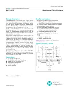
1 MAX1454 Precision Sensor Signal Conditionerwith overvoltage protection 19-5945 Rev 0; 6/11 General DescriptionThe MAX1454 is a highly integrated analog Sensor Signal Conditioner targeted for automotive applications. The device provides amplification, calibration, and tem-perature compensation to enable an overall performance approaching the inherent repeatability of the Sensor . The fully analog Signal path introduces no quantization noise in the output Signal while enabling digitally controlled trimming of the output. Offset and span are calibrated with integrated 16-bit DACs, allowing sensors to be truly device architecture includes a programmable sen-sor excitation, a 32-step programmable-gain amplifier (PGA), a 2K x 8 bits internal flash memory, four 16-bit DACs, and an on-chip temperature Sensor .
2 In addition to offset and span compensation, the device provides a unique temperature-compensation method for offset TC and FSO TC to provide a remarkable degree of flexibility while minimizing manufacturing device is packaged in a 16-pin TSSOP and covers the automotive AEC-Q100 Grade 1 temperature range of -40NC to + SensorsStrain GaugesPressure Calibrators and ControllersResistive Element SensorsHumidity SensorsBenefits and FeaturesS Complete Signal Conditioning in a Single IC Package Provides Amplification, Calibration, and Temperature Compensation Accommodates Sensor Output Sensitivities from 1mV/V to 200mV/V overvoltage protection to 45V Reverse-Voltage protection to 45VS High- Precision Compensation Reduces Downstream Circuit Complexity Fully Analog Signal Path 16-Bit Offset and Span-Calibration Resolution On-Chip Lookup Table Supports Multipoint Calibration Temperature CorrectionS Supports Both Current and Voltage-Bridge ExcitationS Fast 85 s Step ResponseS Sensor Fault DetectionS Simple PCB LayoutS Single-Pin Digital ProgrammingS No External Trim Components RequiredOrdering Information appears at end of data
3 Related parts and recommended products to use with this part, refer to KIT AVAILABLEFor pricing, delivery, and ordering information, please contact Maxim Direct at 1-888-629-4642, or visit Maxim s website at Sensor Signal Conditionerwith overvoltage protection 2 Maxim Integrated(Voltages referenced to GND.)VDD, VDDF .. to + ..-45V to +45 VAll Other Pins .. to Min (VDDX + , 6V)Continuous Power Dissipation (TA = +70NC) 16-Pin TSSOP (derate above +70NC) .. Temperature Range ..-40NC to +125 NCJunction Temperature ..+150 NCStorage Temperature Range ..-65NC to +150 NCLead Temperature (soldering, 10s) .. +300 NCSoldering Temperature (reflow).
4 +260 NCTSSOP Junction-to-Ambient Thermal Resistance (qJA) ..90NC/W Junction-to-Case Thermal Resistance (qJC) ..27NC/WABSOLUTE MAXIMUM RATINGSNote 1: Package thermal resistances were obtained using the method described in JEDEC specification JESD51-7, using a four-layer board. For detailed information on package thermal considerations, refer to beyond those listed under Absolute Maximum Ratings may cause permanent damage to the device. These are stress ratings only, and functional opera-tion of the device at these or any other conditions beyond those indicated in the operational sections of the specifications is not implied.
5 Exposure to absolute maximum rating conditions for extended periods may affect device THERMAL CHARACTERISTICS(Note 1)ELECTRICAL CHARACTERISTICS(VDDX = 5V, VGND = 0V, TA = +25NC, unless otherwise noted.) (Note 2)PARAMETERSYMBOLCONDITIONSMINTYPMAXUNIT SGENERAL CHARACTERISTICSE xternal Supply Supply CurrentIDDX(Note 3) Regulator Output VoltageVDDNot to be loaded by external circuitry, must be connected to a capacitor to ThresholdVPORR eferred to VDDX Supply Voltage-Ramp Rate(Note 4)1V/msANALOG INPUTI nput ImpedanceRIN1 MIInput-Referred Offset-Temperature Coefficient(Notes 5, 6)Q1FV/NCInput-Referred Adjustable-Offset RangeOffset TC = 0 at gain = 44 (Note 7)-150+150mVNonlinearity of Signal PathPercent of 4V span, no load, IRO[3:0] = 0000bin, source impedance = 5kI, VOUT = to.
6 Measured at VOUT = [ , , ] at a gain of Rejection RatioCMRRS pecified for common-mode voltages between GND and VDDX 90dBInput-Referred Adjustable FSO(Note 8)1200mV/VMAX1454 Precision Sensor Signal Conditionerwith overvoltage protection 3 Maxim IntegratedELECTRICAL CHARACTERISTICS (continued)(VDDX = 5V, VGND = 0V, TA = +25NC, unless otherwise noted.) (Note 2)PARAMETERSYMBOLCONDITIONSMINTYPMAXUNIT SANALOG OUTPUTD ifferential Signal GainSelectable in 32 steps6 to 2048V/VPGA[4:0] = [4:0] = [4:0] = 01010bin404448 PGA[4:0] = 01100bin586470 PGA[4:0] = 01101bin728088 PGA[4:0] = 01110bin8696106 PGA[4:0] = 01111bin101112123 PGA[4:0] = 10000bin130144158 PGA[4:0] = 10110bin374416458 PGA[4:0] = 11100bin103711521267 PGA[4.]
7 0] = 11111bin182320482253 Output-Voltage SwingNo loadVGND + - LowIOUT = 1mA sinking, TA = TMIN to HighIOUT = 1mA sourcing, TA = TMIN to TMAXVDDX - Current DriveCapabilityMaintain DC output to 2mV error compared to no load case (Note 4)Q1mAOutput Source Current Limit8mAOutput Sink Current Limit-8mAOutput Impedance at DCVOUT = Offset RatioDVOUT/DOffset Offset TC RatioDVOUT/DOffset TC Response(63% Final Value)85 FsMaximum Capacitive at Output PinDC to 1kHz, source impedance = 5kIGain = = = 5123 Gain = 10246 Gain = 204812 MAX1454 Precision Sensor Signal Conditionerwith overvoltage protection 4 Maxim IntegratedELECTRICAL CHARACTERISTICS (continued)(VDDX = 5V, VGND = 0V, TA = +25NC, unless otherwise noted.)
8 (Note 2)PARAMETERSYMBOLCONDITIONSMINTYPMAXUNIT SBRIDGE DRIVEB ridge RatioAACMRATIO[1:0] = [1:0] = [1:0] = [1:0] = 11243036 Maximum Bridge Load CapacitanceVoltage excitation mode (Note 4)1nFFSO DAC Code Range(Note 4)0x40000xC000 HexOutput Voltage RangeVBDR(Note 4) - CONVERTERS (DACs)DAC Resolution16 BitsOffset DAC Bit WeightDVOUT/DCodeDAC reference = VDDX = 5V76FV/bitOffset TC DAC Bit WeightDVOUT/DCodeDAC reference = VBDR = DAC Bit WeightDVBDR/DCodeDAC reference = VDDX = 5V76FV/bitFSO TC DAC Bit WeightDVBDR/DCodeDAC reference = VBDR = DAC IRO DAC ResolutionIncluding sign5 BitsIRO DAC Bit WeightDVOUT/DCodeInput referred, DAC reference = VDDX = 5V (Note 9)
9 RESISTORSOUT/DIO Pullup ResistanceRPULLUP100kICurrent Source Reference ResistorRISRC10kICurrent Source Reference Resistor Temperature CoefficientTCRISRC600ppm/NCFLASH MEMORYE ndurance(Notes 4, 10)10,000 CyclesRetentionTA = +85NC (Note 4)10 YearsPage Erase Time(Notes 4, 11)32msMass Erase Time(Notes 4, 11)32msMAX1454 Precision Sensor Signal Conditionerwith overvoltage protection 5 Maxim IntegratedELECTRICAL CHARACTERISTICS (continued)(VDDX = 5V, VGND = 0V, TA = +25NC, unless otherwise noted.) (Note 2)Note 2: All units are production tested at TA = +25NC and +125NC. Specifications over temperature are guaranteed by 3: Excludes Sensor or load current.
10 Analog mode with voltage excitation on BDR pin, FSODAC = 4: Specification is guaranteed by design. Note 5: All electronics temperature errors are compensated together with Sensor 6: The Sensor and the device must be at the same temperature during calibration and 7: This is the maximum allowable Sensor 8: This is the Sensor s sensitivity normalized to its drive voltage, assuming a desired full-span output of VDDX - 1V and a nominal bridge voltage of 9: Bit weight is ratiometric to 10: Programming of the flash memory at room temperature is 11: No commands can be executed until the erase operation has completed. During erase operations, all commands sent to the device are Current(Note 4)8mAProgram/Erase Current(Note 4)7mATEMPERATURE-TO-DIGITAL CONVERTERT emperature ADC Digital Output0x00hexHighest Digital Output0xAFhexDIGITAL INPUT (OUT/DIO)Input Low VoltageVIL0 VDDX/3 VInput High VoltageVIHVDDX x 2/3 VDDXVOVERVOLTAGE PROTECTIONO vervoltage- protection DETECTIONIN+/IN- Low Comparator x VBDRVIN+/IN- High Comparator x VBDRVD etection-Threshold AccuracyQ25mVComparator Hysteresis20mVOutput Clip Level During Fault ConditionsIOUT = 1mA sinking150250mVTypical Operating Characteristics(TA = +25 C, unless otherwise noted.)
