Transcription of 2N7002 - Diodes Incorporated
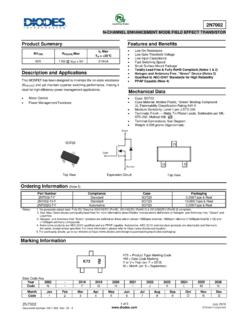
1 2N7002 Document number: DS11303 Rev. 33 - 2 1 of 5 July 2013 Diodes Incorporated 2N7002 N-CHANNEL ENHANCEMENT MODE MOSFET Product Summary V(BR)DSS RDS(ON) max ID max TA = +25 C 60V @ VGS = 5V 210mA Description This MOSFET has been designed to minimize the on-state resistance (RDS(ON)) and yet maintain superior switching performance, making it ideal for high efficiency power management applications. Applications Motor Control Power Management Functions Features Low On-Resistance Low Gate Threshold Voltage Low Input Capacitance Fast Switching Speed Small Surface Mount Package Totally Lead-Free & Fully RoHS Compliant (Notes 1 & 2) Halogen and Antimony Free.
2 Green Device (Notes 3 & 4) Qualified to AEC-Q101 standards for High Reliability Mechanical Data Case: SOT23 Case Material: Molded Plastic, Green Molding Compound. UL Flammability Classification Rating 94V-0 Moisture Sensitivity: Level 1 per J-STD-020 Terminals: Matte Tin Finish annealed over Alloy 42 leadframe (Lead Free Plating). Solderable per MIL-STD-202, Method 208 Terminal Connections: See Diagram Weight: grams (approximate) Ordering Information (Note 5) Part Number Compliance Case Packaging 2N7002 -7-F Standard SOT23 3,000/Tape & Reel 2N7002 -13-F Standard SOT23 10,000/Tape & Reel 2N7002Q-7-F Automotive SOT23 3,000/Tape & Reel Notes: 1.
3 No purposely added lead. Fully EU Directive 2002/95/EC (RoHS) & 2011/65/EU (RoHS 2) compliant. 2. See for more information about Diodes Incorporated s definitions of Halogen- and Antimony-free, "Green" and Lead-free. 3. Halogen- and Antimony-free "Green products are defined as those which contain <900ppm bromine, <900ppm chlorine (<1500ppm total Br + Cl) and <1000ppm antimony compounds. 4. Product manufactured with Date Code V12 (week 50, 2008) and newer are built with Green Molding Compound. Product manufactured prior to Date Code V12 are built with Non-Green Molding Compound and may contain Halogens or Sb2O3 Fire Retardants. 5. For packaging details, go to our website at Marking Information Date Code Key Year 2002 2003 2004 2005 2006 2007 2008 2009 2010 2011 2012 2013 2014 2015 2016 2017 Code N P R S T U V W X Y Z A B C D E Month Jan Feb Mar Apr May Jun Jul Aug Sep Oct Nov Dec Code 1 2 3 4 5 6 7 8 9 O N D SOT23 Top View Equivalent CircuitTop View DGSK72 = Product Type Marking Code YM = Date Code Marking for SAT (Shanghai Assembly/ Test site) = Date Code Marking for CAT (Chengdu Assembly/ Test site) Y or = Year (ex.)
4 A = 2013) M = Month (ex: 9 = September) Shanghai A/T SiteChengdu A/T Site SourceGateDrainYMYK72 YMK72YM 2N7002 Document number: DS11303 Rev. 33 - 2 2 of 5 July 2013 Diodes Incorporated 2N7002 Maximum Ratings (@TA = +25 C, unless otherwise specified.) Characteristic Symbol Value Units Drain-Source Voltage VDSS 60 V Drain-Gate Voltage RGS VDGR 60 V Gate-Source Voltage Continuous Pulsed VGSS 20 40 V Continuous Drain
5 Current (Note 6) VGS = 10V Steady State TA = +25 CTA = +85 C TA = +100 CID 170 120 105 mA Continuous Drain Current (Note 7) VGS = 10V Steady State TA = +25 CTA = +85 C TA = +100 CID 210 150 135 mA Maximum Body diode Forward Current (Note 7) Pulsed Continuous IS 2 A Pulsed Drain Current (10 s pulse, duty cycle = 1%) IDM 800 mA Thermal Characteristics (@TA = +25 C, unless otherwise specified.) Characteristic Symbol Value Units Total Power Dissipation (Note 6) PD 370 mW (Note 7) 540 Thermal Resistance, Junction to Ambient (Note 6) R JA 348 C/W (Note 7) 241 Thermal Resistance, Junction to Case (Note 7) R JC 91 Operating and Storage Temperature Range TJ, TSTG -55 to +150 C Electrical Characteristics (@TA = +25 C, unless otherwise specified.)
6 Characteristic Symbol Min Typ Max Unit Test Condition OFF CHARACTERISTICS (Note 8) Drain-Source Breakdown Voltage BVDSS 60 70 V VGS = 0V, ID = 10 A Zero Gate Voltage Drain Current @ TC = +25 C @ TC = +125 CIDSS 500 A VDS = 60V, VGS = 0V Gate-Body Leakage IGSS 10 nA VGS = 20V, VDS = 0V ON CHARACTERISTICS (Note 8) Gate Threshold Voltage VGS(th) V VDS = VGS, ID = 250 A Static Drain-Source On-Resistance @ TJ = +25 C @ TJ = +25 C @ TJ = +125 CRDS(ON)
7 VGS = , ID = VGS = 10V, ID = VGS = 10V, ID = On-State Drain Current ID(ON) A VGS = 10V, VDS = Forward Transconductance gFS 80 mS VDS =10V, ID = diode Forward Voltage VSD V VGS = 0V, IS = 115mA DYNAMIC CHARACTERISTICS (Note 9) Input Capacitance Ciss 22 50 pF VDS = 25V, VGS = 0V f = Output Capacitance Coss 11 25 pF Reverse Transfer Capacitance Crss pF Gate resistance Rg 120 VDS = 0V, VGS = 0V, f = Total Gate Charge (VGS = ) Qg 223 pC VDS = 10V, ID = 250mA Gate-Source Charge Qgs 82 Gate-Drain Charge Qgd 178 SWITCHING CHARACTERISTICS (Note 9) Turn-On Delay Time tD(on) ns VDD = 30V, ID = , RL = 150 , VGEN = 10V, RGEN = 25 Turn-On Rise Time tr Turn-Off Delay Time tD(off) Turn-Off Fall Time tf Notes: 6.
8 Device mounted on FR-4 PCB, with minimum recommended pad layout 7. Device mounted on 1 x 1 FR-4 PCB with high coverage 2oz. Copper, single sided. 8. Short duration pulse test used to minimize self-heating effect. 9. Guaranteed by design. Not subject to product testing. 2N7002 Document number: DS11303 Rev. 33 - 2 3 of 5 July 2013 Diodes Incorporated 2N7002 2345V , DRAIN-SOURCE VOLTAGE (V)Fig. 1 On-Region CharacteristicsDSI , DRAIN-SOURCE CURRENT (A) , DRAIN CURRENT (A)Fig. 2 On-Resistance vs. Drain , NORMALIZED DRAIN-SOURCE ON-RESISTANCE ( )DS(ON) 145T , JUNCTION TEMPERATURE ( C)Fig. 3 On-Resistance vs. Junction Temperaturej V = 10V,I = 200mAGSDR, STATIC DRAIN-SOURCE ON-RESISTANCE ( )DS(ON) 0V , GATE TO SOURCE VOLTAGE (V)Fig.
9 4 On-Resistance vs. Gate-Source VoltageGSI = 50mAD I = 500mAD 123456024681012141618R, NORMALIZED DRAIN-SOURCE ON-RESISTANCE ( )DS(ON) GATE SOURCE CURRENT (V)GS,I , DRAIN CURRENT (A)Fig. 5 Typical Transfer CharacteristicsD658710905010015020025030 03500255075100125150 175200P, POWER DISSIPATION (mW)dT , AMBIENT TEMPERATURE ( C)Fig. 6 Max Power Dissipation vs. Ambient TemperatureA 400 2N7002 Document number: DS11303 Rev. 33 - 2 4 of 5 July 2013 Diodes Incorporated 2N7002 Package Outline Dimensions Please see AP02002 at for latest version. Suggested Pad Layout Please see AP02001 at for the latest version. SOT23 Dim Min Max Typ A B C D F G H J K K1 - - L M 0 8 - All Dimensions in mm Dimensions Value (in mm) Z X Y C E AMJLDFBCHKGK1 XEYCZ 2N7002 Document number: DS11303 Rev.
10 33 - 2 5 of 5 July 2013 Diodes Incorporated 2N7002 IMPORTANT NOTICE Diodes Incorporated MAKES NO WARRANTY OF ANY KIND, EXPRESS OR IMPLIED, WITH REGARDS TO THIS DOCUMENT, INCLUDING, BUT NOT LIMITED TO, THE IMPLIED WARRANTIES OF MERCHANTABILITY AND FITNESS FOR A PARTICULAR PURPOSE (AND THEIR EQUIVALENTS UNDER THE LAWS OF ANY JURISDICTION). Diodes Incorporated and its subsidiaries reserve the right to make modifications, enhancements, improvements, corrections or other changes without further notice to this document and any product described herein. Diodes Incorporated does not assume any liability arising out of the application or use of this document or any product described herein; neither does Diodes Incorporated convey any license under its patent or trademark rights, nor the rights of others.