Transcription of 300mA, Ultra-Low Noise, Ultra-Fast CMOS LDO Regulator
1 RT9193. 300mA, Ultra-Low Noise, Ultra-Fast CMOS LDO Regulator General Description Features The RT9193 is designed for portable RF and wireless ultra Low Noise for RF Application applications with demanding performance and space ultra Fast Response in Line/Load Transient requirements. The RT9193 performance is optimized for s). Quick Start-Up (Typically 50 . battery-powered systems to deliver ultra low noise and < A Standby Current When Shutdown low quiescent current. A noise bypass pin is available for Low Dropout : 220mV @ 300mA. further reduction of output noise. Regulator ground current wide Operating Voltage Ranges : to increases only slightly in dropout, further prolonging the TTL-Logic-Controlled Shutdown input battery life.
2 The RT9193 also works with low-ESR ceramic Low Temperature Coefficient capacitors, reducing the amount of board space necessary Current Limiting Protection for power applications, critical in hand-held wireless Thermal Shutdown Protection devices. The RT9193 consumes less than A in Only 1 F Output Capacitor Required for Stability shutdown mode and has fast turn-on time less than 50 s. High Power Supply Rejection Ratio The other features include ultra low dropout voltage, high Custom Voltage Available output accuracy, current limiting protection, and high ripple RoHS Compliant and 100% Lead (Pb)-Free rejection ratio. Available in the SC-70-5, SOT-23-5, TSOT-23-5, WDFN-6L 2x2 and MSOP-8 packages.
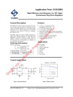
3 Applications CDMA/GSM Cellular Handsets Ordering Information Battery-Powered Equipment RT9193- Laptop, Palmtops, Notebook Computers Package Type Hand-Held Instruments U5 : SC-70-5 PCMCIA Cards B : SOT-23-5. J5 : TSOT-23-5 Portable Information Appliances QW : WDFN-6L 2x2 (W-Type). F : MSOP-8 Marking Information Lead Plating System For marking information, contact our sales representative P : Pb Free G : Green (Halogen Free and Pb Free) directly or through a Richtek distributor located in your area. Output Voltage 15 : 16 : Typical Application Circuit : 49 : 50 : RT9193. 1H : VIN VOUT. VIN VOUT. 2H : CIN COUT. 4G : 1 F/X7R 1 F/X7R. ( to 5V with step is available) GND.
4 Note : Chip Enable EN BP. Richtek products are : CBP. 22nF. RoHS compliant and compatible with the current require- (Option for low noise). ments of IPC/JEDEC J-STD-020. Suitable for use in SnPb or Pb-free soldering processes. Copyright 2016 Richtek Technology Corporation. All rights reserved. is a registered trademark of Richtek Technology Corporation. DS9193-17 January 2016 1. RT9193. Pin Configurations (TOP VIEW). VOUT BP. 5 4 EN 1 6 BP NC 8 NC. VIN 2 7 EN. GND 2 5 NC. 7 NC 3 6 BP. 2 3 VIN 3 4 VOUT VOUT 4 5 GND. VIN GND EN. WDFN-6L 2x2 MSOP-8. SC-70-5/SOT-23-5/TSOT-23-5. Functional Pin Description Pin Name Pin Function Chip Enable (Active High).
5 Note that this pin is high impedance. There should be a pull low 100k . EN. resistor connected to GND when the control signal is floating. Reference Noise Bypass. This pin can be floating. For lowest noise performance, connect a 22nF. BP. capacitor between the BP and GND pins. GND Ground. VOUT Output Voltage. VIN Power input Voltage. Function Block Diagram EN Shutdown VIN. Quick and Start Logic Control BP VREF. + MOSFET. Driver - Error Amplifier VOUT. Current-Limit and Thermal Protection GND. Copyright 2016 Richtek Technology Corporation. All rights reserved. is a registered trademark of Richtek Technology Corporation. DS9193-17 January 2016. 2.
6 RT9193. Absolute Maximum Ratings (Note 1). Supply input Voltage ---------------------------------------- ---------------------------------------- ---------------------- 6V. Power Dissipation, PD @ TA = 25 C. SC-70-5 ---------------------------------------- ---------------------------------------- -------------------------------------- 300mW. TSOT-23-5/SOT-23-5 ---------------------------------------- ---------------------------------------- ---------------------- 400mW. WDFN-6L 2x2 ---------------------------------------- ---------------------------------------- ------------------------------ 606mW. MSOP-8 ---------------------------------------- ---------------------------------------- ------------------------------------- 625mW.
7 Package Thermal Resistance (Note 2). SC-70-5, JA ---------------------------------------- ---------------------------------------- -------------------------------- 333 C/W. SC-70-5, JC ---------------------------------------- ---------------------------------------- -------------------------------- 200 C/W. TSOT-23-5/SOT-23-5, JA ---------------------------------------- ---------------------------------------- ---------------- 250 C/W. TSOT-23-5/SOT-23-5, JC ---------------------------------------- ---------------------------------------- --------------- 25 C/W. WDFN-6L 2x2, JA ---------------------------------------- ---------------------------------------- ------------------------- 165 C/W.
8 WDFN-6L 2x2, JC ---------------------------------------- ---------------------------------------- ------------------------ 20 C/W. MSOP-8 JA ---------------------------------------- ---------------------------------------- -------------------------------- 160 C/W. MSOP-8 JC ---------------------------------------- ---------------------------------------- -------------------------------- 55 C/W. Junction Temperature ---------------------------------------- ---------------------------------------- --------------------- 150 C. Lead Temperature (Soldering, 10 sec.) ---------------------------------------- --------------------------------------- 260 C. Storage Temperature Range ---------------------------------------- ---------------------------------------- ------------ 65 C to 150 C.
9 ESD Susceptibility (Note 3). HBM (Human Body Model) ---------------------------------------- ---------------------------------------- -------------- 2kV. MM (Machine Model) ---------------------------------------- ---------------------------------------- --------------------- 200V. Recommended Operating Conditions (Note 4). Supply input Voltage ---------------------------------------- ---------------------------------------- ---------------------- to EN input Voltage ---------------------------------------- ---------------------------------------- --------------------------- 0V to Junction Temperature Range ---------------------------------------- ---------------------------------------- ------------ 40 C to 125 C.
10 Ambient Temperature Range ---------------------------------------- ---------------------------------------- ------------ 40 C to 85 C. Electrical Characteristics (VIN = VOUT + 1V, CIN = COUT = 1 F, CBP = 22nF, TA = 25 C, unless otherwise specified). Parameter Symbol Test Conditions Min Typ Max Unit Output Voltage Accuracy VOUT IOUT = 1mA 2 -- 2 %. Current Limit ILIM RLOAD = 1 360 400 -- mA. Quiescent Current IQ VEN , IOUT = 0mA -- 90 130 A. IOUT = 200mA, VOUT > 170 200. Dropout Voltage (Note 5) VDROP mV. IOUT = 300mA, VOUT > -- 220 300. VIN = (VOUT + 1V) to , Line Regulation VLINE -- -- %. IOUT = 1mA. Load Regulation VLOAD 1mA IOUT 300mA -- -- %.