Transcription of Low Cost Low Power Instrumentation Amplifier AD620
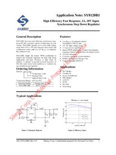
1 Low Cost Low PowerInstrumentation Amplifier AD620 Rev. H Information furnished by Analog Devices is believed to be accurate and reliable. However, no responsibility is assumed by Analog Devices for its use, nor for any infringements of patents or other rights of third parties that may result from its use. Specifications subject to change without notice. No license is granted by implication or otherwise under any patent or patent rights of Analog Devices. Trademarks and registered trademarks are the property of their respective owners. One Technology Way, Box 9106, Norwood, MA 02062-9106, Tel: Fax: 2003 2011 Analog Devices, Inc. All rights reserved. FEATURES Easy to use Gain set with one external resistor (Gain range 1 to 10,000) wide Power supply range ( V to 18 V) Higher performance than 3 op amp IA designs Available in 8-lead DIP and SOIC packaging Low Power , mA max supply current Excellent dc performance (B grade) 50 V max, input offset voltage V/ C max, input offset drift nA max, input bias current 100 dB min common-mode rejection ratio (G = 10) Low noise 9 nV/ Hz @ 1 kHz, input voltage noise V p-p noise ( Hz to 10 Hz) Excellent ac specifications 120 kHz bandwidth (G = 100) 15 s settling time to APPLICATIONS Weigh scales ECG and medical Instrumentation Transducer interface Data acquisition systems Industrial process controls Battery-powered and portable equipment CONNECTION DIAGRAM INRG VS+INRG+VSOUTPUTREF12348765AD620 TOP VIEW00775-0-001 Figure 1.
2 8-Lead PDIP (N), CERDIP (Q), and SOIC (R) Packages PRODUCT DESCRIPTION The AD620 is a low cost, high accuracy Instrumentation Amplifier that requires only one external resistor to set gains of 1 to 10,000. Furthermore, the AD620 features 8-lead SOIC and DIP packaging that is smaller than discrete designs and offers lower Power (only mA max supply current), making it a good fit for battery-powered, portable (or remote) applications. The AD620 , with its high accuracy of 40 ppm maximum nonlinearity, low offset voltage of 50 V max, and offset drift of V/ C max, is ideal for use in precision data acquisition systems, such as weigh scales and transducer interfaces. Furthermore, the low noise, low input bias current, and low Power of the AD620 make it well suited for medical applications, such as ECG and noninvasive blood pressure monitors. The low input bias current of nA max is made possible with the use of Super eta processing in the input stage.
3 The AD620 works well as a preamplifier due to its low input voltage noise of 9 nV/ Hz at 1 kHz, V p-p in the Hz to 10 Hz band, and pA/ Hz input current noise. Also, the AD620 is well suited for multiplexed applications with its settling time of 15 s to , and its cost is low enough to enable designs with one in-amp per channel. Table 1. Next Generation Upgrades for AD620 Part Comment AD8221 Better specs at lower price AD8222 Dual channel or differential out AD8226 Low Power , wide input range AD8220 JFET input AD8228 Best gain accuracy AD8295 +2 precision op amps or differential out AD8429 ultra low noise 0510152030,0005,00010,00015,00020,00025, 0000 TOTAL ERROR, PPM OF FULL SCALESUPPLY CURRENT (mA) AD620 ARG3 OP AMP IN-AMP(3 OP-07s)00775-0-002 Figure 2. Three Op Amp IA Designs vs. AD620 AD620 Rev. H | Page 2 of 20 TABLE OF CONTENTS Absolute Maximum ESD Typical Performance Theory of Gain input and Output Offset Reference input RF Common-Mode Ground Returns for input Bias AD620 ACHIPS Outline Ordering REVISION HISTORY 7/11 Rev.
4 G to Rev. H Deleted Figure Added Table 1 ..1 Moved Figure 2 ..1 Added ESD input Diodes to Simplified Schematic ..12 Changes to input Protection Added Figure 41; Renumbered Sequentially ..15 Changes to AD620 ACHIPS Information Section ..18 Updated Ordering Guide ..20 12/04 Rev. F to Rev. G Updated Universal Change to Features ..1 Change to Product Changes to Added Metallization Replaced Figure 4-Figure 6 ..6 Replaced Figure 15 ..7 Replaced Figure 33 ..10 Replaced Figure 34 and Figure 35 ..10 Replaced Figure 37 ..10 Changes to Table 3 ..13 Changes to Figure 41 and Figure 42 ..14 Changes to Figure 43 ..15 Change to Figure 44 ..17 Changes to input Protection section ..15 Deleted Figure 9 ..15 Changes to RF Interference section ..15 Edit to Ground Returns for input Bias Currents Added AD620 CHIPS to Ordering Guide ..19 7/03 Data Sheet Changed from Rev. E to Rev. F Edit to 1 Changes to SPECIFICATIONS.
5 2 Removed AD620 CHIPS from ORDERING GUIDE .. 4 Removed METALLIZATION 4 Replaced TPCs 1 3 .. 5 Replaced TPC 12 .. 6 Replaced TPC 30 .. 9 Replaced TPCs 31 and Replaced Figure 4 ..10 Changes to Table I ..11 Changes to Figures 6 and 7 ..12 Changes to Figure 8 ..13 Edited input PROTECTION section ..13 Added new Figure 9 ..13 Changes to RF INTERFACE section ..14 Edit to GROUND RETURNS FOR input BIAS CURRENTS Updated OUTLINE DIMENSIONS ..16 AD620 Rev. H | Page 3 of 20 SPECIFICATIONS Typical @ 25 C, VS = 15 V, and RL = 2 k , unless otherwise noted. Table 2. Parameter Conditions AD620A AD620B AD620S1 Min Typ Max Min Typ Max Min Typ Max Unit GAIN G = 1 + ( k /RG) Gain Range 1 10,000 1 10,000 1 10,000 Gain Error2 VOUT = 10 V G = 1 % G = 10 % G = 100 % G = 1000 % Nonlinearity VOUT = 10 V to +10 V G = 1 1000 RL = 10 k 10 40 10 40 10 40 ppm G = 1 100 RL = 2 k 10 95 10 95 10 95 ppm Gain vs.
6 Temperature G = 1 10 10 10 ppm/ C Gain >12 50 50 50 ppm/ C VOLTAGE OFFSET (Total RTI Error = VOSI + VOSO/G) input Offset, VOSI VS = 5 V to 15 V 30 125 15 50 30 125 V Overtemperature VS = 5 V to 15 V 185 85 225 V Average TC VS = 5 V to 15 V V/ C Output Offset, VOSO VS = 15 V 400 1000 200 500 400 1000 V VS = 5 V 1500 750 1500 V Overtemperature VS = 5 V to 15 V 2000 1000 2000 V Average TC VS = 5 V to 15 V 15 15 V/ C Offset Referred to the input vs. Supply (PSR) VS = V to 18 V G = 1 80 100 80 100 80 100 dB G = 10 95 120 100 120 95 120 dB G = 100 110 140 120 140 110 140 dB G = 1000 110 140 120 140 110 140 dB input CURRENT input Bias Current 2 nA Overtemperature 4 nA Average TC pA/ C input Offset Current nA Overtemperature nA Average TC pA/ C input input Impedance Differential 10||2 10||2 10||2 G _pF Common-Mode 10||2 10||2 10||2 G _pF input Voltage Range3 VS = V to 5 V VS + +VS VS + +VS VS + +VS V Overtemperature VS + +VS VS + +VS VS + +VS V VS = 5 V to 18 V VS + +VS VS + +VS VS + +VS V Overtemperature VS + +VS VS
7 + +VS + VS + +VS V AD620 Rev. H | Page 4 of 20 AD620A AD620B AD620S1 Parameter Conditions Min Typ Max Min Typ Max Min Typ Max Unit Common-Mode Rejection Ratio DC to 60 Hz with 1 k Source Imbalance VCM = 0 V to 10 V G = 1 73 90 80 90 73 90 dB G = 10 93 110 100 110 93 110 dB G = 100 110 130 120 130 110 130 dB G = 1000 110 130 120 130 110 130 dB OUTPUT Output Swing RL = 10 k VS = V to 5 V VS + +VS VS + +VS VS + +VS V Overtemperature VS +
8 +VS VS + +VS VS + +VS V VS = 5 V to 18 V VS + +VS VS + +VS VS + +VS V Overtemperature VS + +VS VS + +VS VS + +VS V Short Circuit Current 18 18 18 mA DYNAMIC RESPONSE Small Signal 3 dB Bandwidth G = 1 1000 1000 1000 kHz G = 10 800 800 800 kHz G = 100 120 120 120 kHz G = 1000 12 12 12 kHz Slew Rate V/ s Settling Time to 10 V Step G = 1 100 15 15 15 s G = 1000 150 150 150 s NOISE Voltage Noise, 1 kHz 22)/()
9 (GeeNoiseRTIT otalnoni+= input , Voltage Noise, eni 9 13 9 13 9 13 nV/ Hz Output, Voltage Noise, eno 72 100 72 100 72 100 nV/ HzRTI, Hz to 10 Hz G = 1 V p-p G = 10 V p-p G = 100 1000 V p-p Current Noise f = 1 kHz 100 100 100 fA/ Hz Hz to 10 Hz 10 10 10 pA p-p REFERENCE input RIN 20 20 20 k IIN VIN+, VREF = 0 50 60 50 60 50 60 A Voltage Range VS + +VS VS + +VS VS + +VS V Gain to Output 1 1 1 Power SUPPLY Operating Range4 18 18 18 V Quiescent Current VS = V to 18 V mA Overtemperature mA TEMPERATURE RANGE)
10 For Specified Performance 40 to +85 40 to +85 55 to +125 C 1 See Analog Devices military data sheet for 883B tested specifications. 2 Does not include effects of external resistor RG. 3 One input grounded. G = 1. 4 This is defined as the same supply range that is used to specify PSR. AD620 Rev. H | Page 5 of 20 ABSOLUTE MAXIMUM RATINGS Table 3. Parameter Rating Supply Voltage 18 V Internal Power Dissipation1 650 mW input Voltage (Common-Mode) VS Differential input Voltage 25 V Output Short-Circuit Duration Indefinite Storage Temperature Range (Q) 65 C to +150 C Storage Temperature Range (N, R) 65 C to +125 C Operating Temperature Range AD620 (A, B) 40 C to +85 C AD620 (S) 55 C to +125 C Lead Temperature Range (Soldering 10 seconds) 300 C 1 Specification is for device in free air: 8-Lead Plastic Package: JA = 95 C 8-Lead CERDIP Package: JA = 110 C 8-Lead SOIC Package.