Transcription of 500mA, Low Dropout, Low Noise Ultra-Fast Without Bypass ...
1 RT90131DS9013-10 April ConfigurationsApplicationszCDMA/GSM Cellular HandsetszPortable Information ApplianceszLaptop, Palmtops, Notebook ComputerszHand-Held InstrumentszMini PCI & PCI-Express Cardsz PCMCIA & New Cards500mA, Low dropout , Low Noise Ultra-Fast WithoutBypass Capacitor CMOS LDO RegulatorOrdering InformationMarking InformationFor marking information, contact our sales representativedirectly or through a Richtek distributor located in DescriptionThe RT9013 is a high-performance, 500mA LDO regulator,offering extremely high PSRR and ultra-low dropout . Idealfor portable RF and wireless applications with demandingperformance and space RT9013 quiescent current as low as 25 A, furtherprolonging the battery life. The RT9013 also works withlow-ESR ceramic capacitors, reducing the amount of boardspace necessary for power applications, critical in hand-held wireless RT9013 consumes typical A in shutdown modeand has fast turn-on time less than 40 s.
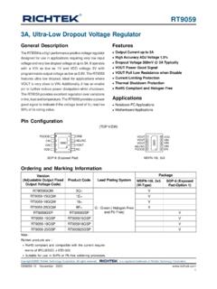
2 The other featuresinclude ultra-low dropout voltage, high output accuracy,current limiting protection, and high ripple rejection in the SC-82, SOT-23-5, SC-70-5 and WDFN-6L2x2 package.(TOP VIEW)WDFN-6L 2x2 FeatureszzzzzWide Operating Voltage Ranges : to dropout : 250mV at 500mAzzzzzUltra-Low- Noise for RF ApplicationzzzzzUltra-Fast Response in Line/Load TransientzzzzzCurrent Limiting ProtectionzzzzzThermal Shutdown ProtectionzzzzzHigh Power Supply Rejection RatiozzzzzOutput Only 1 F Capacitor Required for StabilityzzzzzTTL-Logic-Controlled Shutdown InputzzzzzRoHS Compliant and 100% Lead (Pb)-FreeSOT-23-5 / SC-70-5 Note :Richtek products are :` RoHS compliant and compatible with the current require- ments of IPC/JEDEC J-STD-020.` Suitable for use in SnPb or Pb-free soldering GND ENVOUTNC4235 ENGNDNCNCVOUTVIN541236 GND7 VINVOUTENGND324SC-82RT9013 Package TypeY : SC-82B : SOT-23-5U5 : SC-70-5QW : WDFN-6L 2x2 (W-Type)Lead Plating SystemP : Pb FreeG : Green (Halogen Free and Pb Free)Fixed Output Voltage12 : : : : :32 : : : : : April Application CircuitFunctional Pin DescriptionPin Number SC-82 SOT-23-5 / SC-70-5 WDFN-6L 2x2 Pin Name Pin Function 3 5 4 VOUT Regulator Output.
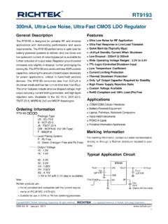
3 -- 4 5, 6 NC No Internal Connection. 2 2 2, 7 (Exposed Pad) GND Common Ground. The exposed pad must be soldered to a large PCB and connected to GND for maximum power dissipation. 1 3 1 EN Enable Input Logic, Active High. When the EN goes to a logic low, the device will be shutdown mode. 4 1 3 VIN Supply Input. Function Block Diagram+-POROTPENVINVOUTGNDMOSD riverCurrentLimitVREFVINGNDVOUTRT9013 COUT1 F/X7R1 F/X7 RNCENCINVINVOUTChip Enable Rpull_down100kRT90133DS9013-10 April Maximum Ratings (Note 1)zSupply Input Voltage--------------------------------- ---------------------------------------- ----------------------------- 6 VzEN Input Voltage--------------------------------- ---------------------------------------- ---------------------------------- 6 VzPower Dissipation, PD @ TA = 25 CSOT-23-5------------------------------- ---------------------------------------- ---------------------------------------- ----- SC-82----------------------------------- ---------------------------------------- --------------------------------- 2x2 Thermal Resistance (Note 2)
4 SOT-23-5, JA-------------------------------------- ---------------------------------------- --------------------------------- 250 C/WSOT-23-5, JC-------------------------------------- ---------------------------------------- -------------------------------- 25 C/WSC-70-5/ SC-82, JA-------------------------------------- ---------------------------------------- ------------------------ 333 C/WWDFN-6L 2x2, JA-------------------------------------- ---------------------------------------- --------------------------- 165 C/WWDFN-6L 2x2, JC-------------------------------------- ---------------------------------------- --------------------------- 20 C/WzLead Temperature (Soldering, 10 sec.) ---------------------------------------- --------------------------------------- 260 CzJunction Temperature----------------------------- ---------------------------------------- -------------------------------- 150 CzStorage Temperature Range----------------------------------- ---------------------------------------- ----------------- 65 C to 150 CzESD Susceptibility (Note 3)HBM ---------------------------------------- ---------------------------------------- ---------------------------------------- -- 2kVMM ---------------------------------------- ---------------------------------------- ---------------------------------------- ---- 200 VRecommended Operating Conditions (Note 4)
5 ZSupply Input Voltage--------------------------------- ---------------------------------------- ----------------------------- to Temperature Range----------------------------------- ---------------------------------------- ----------------- 40 C to 125 CzAmbient Temperature Range----------------------------------- ---------------------------------------- ----------------- 40 C to 85 CElectrical CharacteristicsParameter Symbol Test Conditions Min Typ Max Unit Input Voltage Range VIN -- V Output Noise Voltage VON VOUT = , COUT = 1 F, IOUT = 0mA -- 30 -- VRMS Output Voltage Accur acy (Fixed Output Voltage) VOUT IOUT = 10mA 2 0 +2 % Quiescent Current (Note 5) IQ VEN = 5V, IOUT = 0mA -- 25 50 A Shutdown Current ISHDN VEN = 0V -- A RLOAD = 0 , VIN < A Current Limit ILIM RLOAD = 0 , VIN A IOUT = 400mA, VIN < -- 160 320 dropout Voltage (Note 6) VDROP IOUT = 500mA, VIN -- 250 400 mV 1mA < IOUT < 400 mA VIN < -- -- Load Regulation (Note 7) (Fixed Output Voltage) VLOAD 1mA < IOUT < 500 mA VIN -- -- 1 % (VIN = VOUT + , VEN = VIN, CIN = COUT = 1 F (Ceramic, X7R), TA = 25 C unless otherwise specified)
6 To be continuedRT90134DS9013-10 April 1. Stresses listed as the above Absolute Maximum Ratings may cause permanent damage to the device. These are forstress ratings. Functional operation of the device at these or any other conditions beyond those indicated in the operationalsections of the specifications is not implied. Exposure to absolute maximum rating conditions for extended periods mayremain possibility to affect device 2. JA is measured in the natural convection at TA = 25 C on a low effective thermal conductivity test board of JEDEC 51-3thermal measurement standard. The case position of JC is on the exposed pad for the 3. Devices are ESD sensitive. Handling precaution is 4. The device is not guaranteed to function outside its operating 5.
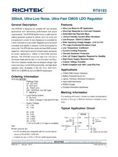
7 Quiescent, or ground current, is the difference between input and output currents. It is defined by IQ = IIN - IOUT under noload condition (IOUT = 0mA). The total current drawn from the supply is the sum of the load current plus the ground 6. The dropout voltage is defined as VIN -VOUT, which is measured when VOUT is VOUT(NORMAL) - 7. Regulation is measured at constant junction temperature by using a 2ms current pulse. Devices are tested for loadregulation in the load range from 10mA to Symbol Test Conditions Min Typ Max Unit Logic-Low VIL 0 -- EN Threshold Voltage Logic-High VIH -- V Enable Pin Current IEN -- 1 A Power Supply Rejection Rate PSRR IOUT = 100mA, f = 10kHz -- 50 -- dB Line Regulation VLINE VIN = (VOUT+ ) to , IOUT = 1mA -- %/V Thermal Shutdown Temperature TSD -- 170 -- Thermal Shutdown Hysteresis TSD -- 30 -- C RT90135DS9013-10 April Operating CharacteristicsOutput Voltage vs.
8 Voltage (V)VIN = ( C)(CIN = COUT = 1 /X7R, unless otherwise specified) dropout Voltage vs. Load Current050100150200250300350050 100 150 200 250 300 350 400 450 500 Load Current (mA) dropout Voltage (mV)RT9013-33 PQWTJ = 125 CTJ = 25 CTJ = -40 CVIN = , ILOAD = 75mAStart UpTime (5 s/Div)EN Pin Voltage(V)Output Voltage(V) = , ILOAD = 50mAEN Pin Shutdown ResponseEN Pin Voltage(V)Time (100 s/Div)Output Voltage(V)420210RT9013-15 PQWQ uiescent Current vs. Temperature1012141618202224262830-50-250 255075100125 TemperatureQuiescent Current (uA)VIN = ( C) dropout Voltage vs. Load Current050100150200250300350050 100 150 200 250 300 350 400 450 500 Load Current (mA) dropout Voltage (mV)RT9013-25 PQWTJ = 125 CTJ = 25 CTJ = -40 CRT90136DS9013-10 April = , ILOAD = 10mA to 100mALoad Transient ResponseLoad Current (mA)Time (100 s/Div)Output VoltageDeviation (mV)100500500-50RT9013-15 PQWVIN = to , ILOAD = 10mALine Transient ResponseInput VoltageDeviation (V)Time (100 s/Div)Output VoltageDeviation (mV) Transient ResponseInput VoltageDeviation (V)Time (100 s/Div)Output VoltageDeviation (mV) = to , ILOAD = 100mART9013-15 PQWVIN = (By Battery), ILOAD = 10mANoiseTime (10ms/Div) Noise ( V/Div)3002001000-100-200-300RT9013-15 PQWVIN = (By Battery), No LoadNoiseTime (10ms/Div) Noise ( V/Div)
9 3002001000-100-200-300RT9013-15 PQWVIN = , ILOAD = 10mA to 300mALoad Transient ResponseLoad Current (mA)Time (100 s/Div)Output VoltageDeviation (mV)4002000500-50RT9013-15 PQWRT90137DS9013-10 April (Hz)PSRR(dB)ILOAD = 100mAILOAD = 300mAILOAD = 10mAVIN = to = (By Battery), ILOAD = 300mANoiseTime (10ms/Div) Noise ( V/Div)3002001000-100-200-300RT9013-15 PQWRT90138DS9013-10 April InformationLike any low- dropout regulator, the external capacitors usedwith the RT9013 must be carefully selected for regulatorstability and performance. Using a capacitor whose valueis > 1 F/X7R on the RT9013 input and the amount ofcapacitance can be increased Without limit. The inputcapacitor must be located a distance of not more than from the input pin of the IC and returned to a cleananalog ground.
10 Any good quality ceramic can be used forthis capacitor. The capacitor with larger value and lowerESR (equivalent series resistance) provides better PSRRand line-transient output capacitor must meet both requirements forminimum amount of capacitance and ESR in all LDOsapplication. The RT9013 is designed specifically to workwith low ESR ceramic output capacitor in space-savingand performance consideration. Using a ceramic capacitorwhose value is at least 1 F with ESR is > 5m on theRT9013 output ensures stability. The RT9013 still workswell with output capacitor of other types due to the widestable ESR range. Figure 1. shows the curves of allowableESR range as a function of load current for various outputcapacitor values. Output capacitor of larger capacitancecan reduce Noise and improve load transient response,stability, and PSRR.