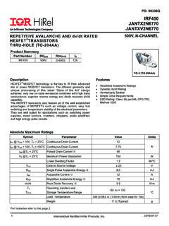
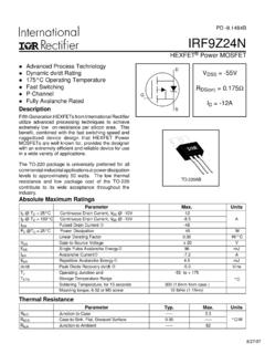
Transcription of Application Note AN-941
1 AN-941 1 Application Note AN-941 PARALLELING POWER MOSFETs Table of Contents Page General observations .. 2 Unbalances due to circuit layout .. 2 Gate oscillations .. 4 Current unbalances in steady-state operation .. 5 Dynamic sharing at turn-on .. 5 Dynamic sharing at turn-off .. 8 In summary .. 9 Appendix .. 11 Abstract: Whenever devices are operated in parallel, due consideration should be given to the sharing between devic-es to ensure that the individual units are operated within their limits.
2 Items that must be considered to suc-cessfully parallel MOSFETs are: gate circuitry, layout considerations, current unbalance, and temperature unbalance. This Application note covers these topics and provides guidelines on paralleling. AN-941 2 General observations Paralleling reduces conduction losses and junction-to-case thermal resistance. However, switching losses remain the same, or may even increase.
3 If they are the dominant losses, only a thermal resistance improvement will be achieved by paralleling. Paralleling to take advantage of lower price of smaller devices should not be attempted without due consider-ation of the technical risks. It is a good engineering practice when paralleling semiconductors to obtain experimental re-sults at the extremes of the manufacturing tolerances. Paralleling of multiple discretes requires that power losses and, more importantly, junction temperatures of each device be equalized as much as possible. Some unbalance of losses is inevitable because of differences in electrical character-istics between different devices.
4 This will require a certain amount of current de-rating, typically around 20%. Even with this de-rating tight thermal coupling is necessary to ensure that individual junction temperatures stay close to each other. The isolation pad that is normally placed between the package and the sink tends to decouple junction tem-peratures and increases temperature differentials. From this point of view, the worst possible mounting method would be to place the paralleled devices on separate heatsinks. A common heatspreader is a very effective way of keeping the semiconductors at the same temperature.
5 It also serves as a mechanical carrier during assembly. If electrical isolation is required the isolation barrier can be placed between the carrier and the heatsink. Unbalances due to circuit layout External circuit unbalance due to non-symmetrical layout can cause significant differences in losses between paralleled devices. The most serious effects of non-symmetrical layout is the current unbalance during switching intervals and the resulting unbalance in switching losses. This will be discussed in more detail in the following sections. Generally speaking, voltage equality is ensured by the fact that the devices are in parallel.
6 However, under transient con-ditions, voltage differentials can appear across devices due to di/dt effects in unequalized stray inductances. The most serious stray circuit element to be balanced is the inductance in series with the source that is common to the gate circuit ( common source inductance ; see Figure 1). The voltage that develops across this inductance due to the di/dt at turn-on and turn-off counteracts the applied gate drive voltage and slows down the rate of change of the source current. AN-941 3 Figure 1.
7 Common Source Inductance If switching losses are relatively small in relation to conduction losses, a certain amount of circuit-induced unbalance of switching losses can be tolerated and layout will not be super-critical. In this case, the simple in-line arrangement that is frequently used can be satisfactory, even though not symmetrical. See Figure 2(A). If switching losses are significant, careful attention to layout is important. The circular layout shown in Figure 2(B) is much superior in terms of balancing common source inductances and equalizing switching losses.
8 Individual stray inductances that are in series with the drain are of lesser concern. An unbalance of 10% in these stray inductances, combined with a di/dt unbalance of 10% translates in an unbalance of 20% in the overshoot seen at turn-off (81 vs. 121V). See Figure 1. However, if the overshoot does not violate the ratings of the MOSFET, the differential in turn-off losses is negligible. The layout of Figure 2(B) will equalize the stray inductances and associated overshoot. Dif-ferences in di/dt are generally contained and do not impact switching energy in a significant way.
9 V+POWER GROUNDGATE A/nsCOMMON SOURCE INDUCTANCE`121V81V AN-941 4 Figure 2 (A) and (B). Different Layouts Gate oscillations It is common knowledge that paralleled MOSFETs must have individual gate resistors. As shown in Figure 3, paralleled MOSFETs have a common low impedance path that is prone to parasitic self oscillations. This is analyzed in greater detail in Ref [1]. Individual gate resistors provide the necessary damping and gate decoupling to prevent oscillations.
10 Figure 3. Low impedance path for parasitic oscillation AN-941 5 Excessive amounts of gate resistance degrade the switching performance of the devices and increase switching unbal-ance. Only the required amount should be used. Current unbalances in steady state operation During the periods outside of the switching transitions, the current in a parallel group of MOSFETs distributes itself in the individual devices in inverse proportion to their on-resistance.