Transcription of Basys3 ™ FPGA Board Reference Manual - Xilinx
1 Basys3 FPGA Board Reference ManualBasys3 rev. C; Revised June 27, 2014 DOC#:502-183 Other product and Overview The Basys3 Board is a complete, readycircuit development platform based on the latest Artix-7 Field Programmable Gate Array (FPGA) from Xilinx . With its high-capacity FPGA ( Xilinx part number XC7A35T-1 CPG236C), low overall cost, collection of USB, VGA, and other ports, the can host designs ranging from introductory combinational circuits to complex sequential circuits like embedded processors and controllersallow a large number designs to be completed without the need for any additional hardware, and enough uncommitted FPGA I/O pins to allow designs to be expanded using Digilent Pmods or custom boards and circuits. The Artix-7 FPGA is optimized for high performance logic, anand more resources than earlier designs. Artix 33,280 logic cells in 5200 slices (each slice contains 1,800 Kbits of fast block RAM Five clock management tiles, each with 90 DSP slices; Internal clock speeds exceeding 450 MHz On-chip analog-to-digital converter (XADC)The Basys3 also offers an improved collection of ports and peripherals, including: 16 user switches 4-digit 7-segment display 12-bit VGA output Digilent USB- jtag port for FPGA programming and communication The Basys3 works with Xilinx s new hightools and design flows that facilitate and enhance the latest design methods.)
2 It runs faster, allows better use of FPGA resources, and allows designers to focus their time evaluating design alternativesSystem Edition includes an on-chip logic analyzer, highand the free Webpack version allows FPGA Board Reference Manual DRAFTJune 27, 2014 Copyright Digilent, Inc. All rights reserved. and company names mentioned may be trademarks of their respective owners. Board is a complete, ready-to-use digital circuit development platform based on the latest 7 Field Programmable Gate Array (FPGA) capacity FPGA ( Xilinx part low overall cost, and , and other ports, the Basys3 can host designs ranging from introductory complex sequential circuits and controllers. It includes enough switches, LEDs and other I/O devices to esigns to be completed without the need for any additional hardware, and enough uncommitted FPGA I/O pins to allow designs to be expanded using Digilent Pmods or 7 FPGA is optimized for high performance logic, and offers more capacity, higher performancehan earlier designs.)
3 Artix-7 35T features include: 33,280 logic cells in 5200 slices (each slice contains four 6-input LUTs and 8 flip-flopsKbits of fast block RAM; ement tiles, each with a phase-locked loop (PLL); Internal clock speeds exceeding 450 MHz; digital converter (XADC). also offers an improved collection of ports and peripherals, including: 16 user LEDs 5 user pushbuttons Three Pmod connectors Pmod for XADC signals USB-UART Bridge Serial Flash USB HID Host for mice, keyboards and memory sticks with Xilinx s new high-performance Vivado Design Suite. Vivado includes many newtools and design flows that facilitate and enhance the latest design methods. It runs faster, allows better designers to focus their time evaluating design alternativeschip logic analyzer, high-level synthesis tool, and other cuttingallows Basys3 designs to be created at no additional Henley Court Pullman, WA 99163 DRAFT Page 1 of 19 It includes enough switches, LEDs and other I/O devices to esigns to be completed without the need for any additional hardware, and enough uncommitted FPGA I/O pins to allow designs to be expanded using Digilent Pmods or other d offers more capacity, higher performance, flops); 5 user pushbuttons Pmod for XADC signals Serial Flash.
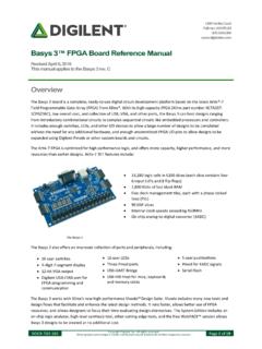
4 Vivado includes many new tools and design flows that facilitate and enhance the latest design methods. It runs faster, allows better designers to focus their time evaluating design alternatives. The cutting-edge tools, l cost. Basys3 FPGA Board Reference Manual Copyright Digilent, Inc. All rights reserved. Other product and company names mentioned may be trademarks of their respective owners. Page 2 of 19 Figure 1. Basys3 Board features A growing collection of Board support IP, Reference designs, and add-on boards are available on the Digilent website. See the Basys3 page at for more information. 1 Power Supplies The Basys3 Board can receive power from the Digilent USB- jtag port (J4) or from a 5 volt external power supply. Jumper JP3 (near the power switch) determines which source is used. All Basys3 power supplies can be turned on and off by a single logic-level power switch (SW16). A power-good LED (LD20), driven by the power good output of the LTC3633 supply, indicates that the supplies are turned on and operating normally.
5 An overview of the Basys3 power circuit is shown in Fig 2. Callout Component Description Callout Component Description 1 Power good LED 9 FPGA configuration reset button 2 Pmod connector(s) 10 Programming mode jumper 3 Analog signal Pmod connector (XADC) 11 USB host connector 4 Four digit 7-segment display 12 VGA connector 5 Slide switches (16) 13 Shared UART/ jtag USB port 6 LEDs (16) 14 External power connector 7 Pushbuttons (5) 15 Power Switch 8 FPGA programming done LED 16 Power Select Jumper Basys3 FPGA Board Reference Manual Copyright Digilent, Inc. All rights reserved. Other product and company names mentioned may be trademarks of their respective owners. Page 3 of 19 Figure 2. Basys 3 Power Circuit The USB port can deliver enough power for the vast majority of designs. A few demanding applications, including any that drive multiple peripheral boards, might require more power than the USB port can provide. Also, some applications may need to run without being connected to a PC s USB port.
6 In these instances an external power supply or battery pack can be used. An external power supply can be used by plugging into the external power header (J6) and setting jumper JP2 to EXT . The supply must deliver to and at least 1A of current ( , at least 5W of power). Many suitable supplies can be purchased through Digikey or other catalog vendors. An external battery pack can be used by connecting the battery s positive terminal to the EXT pin of J6 and the negative terminal to the GND pin of J6. The power provided to USB devices that are connected to Host connector J2 is not regulated. Therefore it is necessary to limit the maximum voltage of an external battery pack to DC. The minimum voltage of the battery pack depends on the application -if the USB Host function (J2) is used, at least needs to be provided. In other cases the minimum voltage is Voltage regulator circuits from Linear Technology create the required , , and supplies from the main power input.
7 Table 2 provides additional information (typical currents depend strongly on FPGA configuration and the values provided are typical of medium size/speed designs). Supply Circuits Device Current (max/typical) FPGA I/O, USB ports, Clocks, Flash, PMODs IC10: LTC3633 2 to FPGA Core IC10: LTC3633 2A/ to FPGA Auxiliary and Ram IC11: LTC3621 300mA/ to Table 2. Basys3 Power Supplies Basys3 FPGA Board Reference Manual Copyright Digilent, Inc. All rights reserved. Other product and company names mentioned may be trademarks of their respective owners. Page 4 of 19 2 FPGA Configuration After power-on, the Artix-7 FPGA must be configured (or programmed) before it can perform any functions. You can configure the FPGA in one of four ways: 1. A PC can use the Digilent USB- jtag circuitry (portJ4, labeled PROG ) to program the FPGA any time the power is on. 2. A file stored in the nonvolatile serial (SPI) flash device can be transferred to the FPGA using the SPI port.
8 3. A programming file can be transferred from a USB memory stick attached to the USB HID port. Figure 3 shows the different options available for configuring the FPGA. An on- Board mode jumper (JP1) selects between the programming modes. The FPGA configuration data is stored in files called bitstreams that have the .bit file extension. The Vivado software from Xilinx can create bitstreams from VHDL, Verilog, or schematic-based source files. Bitstreams are stored in SRAM-based memory cells within the FPGA. This data defines the FPGA s logic functions and circuit connections, and it remains valid until it is erased by removing Board power, by pressing the reset button attached to the PROG input, or by writing a new configuration file using the jtag port. An Artix-7 35T bitstream is typically 17,536,096 bits and can take a long time to transfer. The time it takes to program the Basys3 can be decreased by compressing the bitstream before programming, and then allowing the FPGA to decompress the bitsream itself during configuration.
9 Depending on design complexity, compression ratios of 10x can be achieved. Bitstream compression can be enabled within the Xilinx tools (Vivado) to occur during generation. For instructions on how to do this, consult the Xilinx documentation for the toolset being used. After being successfully programmed, the FPGA will cause the "DONE" LED to illuminate. Pressing the PROG button at any time will reset the configuration memory in the FPGA. After being reset, the FPGA will immediately attempt to reprogram itself from whatever method has been selected by the programming mode jumper. The following sections provide greater detail about programming the Basys3 using the different methods available. Figure 3. Basys3 Configuration Options Basys3 FPGA Board Reference Manual Copyright Digilent, Inc. All rights reserved. Other product and company names mentioned may be trademarks of their respective owners. Page 5 of 19 jtag Programming The Xilinx tools typically communicate with FPGAs using the Test Access Port and Boundary-Scan Architecture, commonly referred to as jtag .
10 During jtag programming, a .bit file is transferred from the PC to the FPGA using the onboard Digilent USB- jtag circuitry (port J4) or an external jtag programmer, such as the Digilent jtag -HS2, attached to port J5 (located below port JA). You can perform jtag programming any time after the Basys3 has been powered on, regardless of what the mode jumper (JP1) is set to. If the FPGA is already configured, then the existing configuration is overwritten with the bitstream being transmitted over jtag . Setting the mode jumper to the jtag setting (seen in Fig 3) is useful to prevent the FPGA from being configured from any other bitstream source until a jtag programming occurs. Programming the Basys3 with an uncompressed bitstream using the on- Board USB_JTAG circuitry usually takes around five seconds. jtag programming can be done using the hardware server in Vivado. The demonstration project available at provides an in depth tutorial on how to program your Board .