Transcription of BOOST/BUCK-BOOST/BUCK/CONTROLLER IC with External …
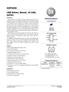
1 Tm TE. CH Preliminary T8332AD. BOOST/BUCK-BOOST/BUCK/CONTROLLER IC with External MOSFET. FEATURES GENERAL DESCRIPTION. 5 - 60V input voltage range The T8332AD is designed to operate as a Single resistor programmable constant constant current source for driving high current current driver LEDs. It is a current mode control IC which Excellent constant current accuracy 3% provides a good line transient response. The typically device can provide an excellent constant current feedback reference voltage tailor- accuracy of +/-3% typically. Moreover, the IC. made for LED application also provide several protection features like IC. Support boost /Buck/Buck- boost overvoltage protection, cycle by cycle current configuration limit protection and thermal shutdown DC Dimming & PWM dimming protection. On-chip thermal shutdown at 170oC. Fixed switching frequency 430kHz Dithering in oscillator frequency to PART NUMBER EXAMPLES.
2 Simplify the EMI design Cycle-by-cycle current limit Over-current protection PART NO. PACKAGE. IC overvoltage protection 15 A shutdown current T8332AD SO8-EP. SO8-EP package Applications High Power LED Driver LED illuminance LCD backlight illumination Automotive interior lighting Automotive Headlights PIN ARRANGEMENT. SO8-EP Version (T8332AD 9 PINS). TM Technology, Inc. reserves the right P. 1 Publication Date: 2017. to change products or specifications without notice. Revision:A tm TE. CH Preliminary T8332AD. TYPICAL APPLICATION. (BUCK- boost ). TM Technology, Inc. reserves the right P. 2 Publication 2017. to change products or specifications without notice. Revision:A tm TE. CH Preliminary T8332AD. PIN DESCRIPTION. T8332AD 9 PINS. Pin No. Pin Name Pin Description 1 DIM DC Dimming Function pin. 2 COMP Compensation pin. Connect a resistor for the current mode control and cycle by 3 CS. cycle current limit function.
3 4 GATE Switch gate drive 5 VREG Internal regulator 6 VIN Main supply 7 VSN Load current sense ve input 8 EN Enable the chip 9 GND Ground Pin. IC ground.(Package EP). TM Technology, Inc. reserves the right P. 3 Publication 2017. to change products or specifications without notice. Revision:A tm TE. CH Preliminary T8332AD. ABSOLUTE MAXIMUM RATINGS. Parameter Symbol Value Unit VIN pin voltage relative to GND to +60 V. DIM pin voltage relative to GND to + V. GATE to +10 V. VSN VIN - 1 V. VREG to +8 V. COMP ENand CS pin voltage to + V. relative to GND. o Junction temperature range TJ -40 to +150 C. Maximum soldering temperature o TLEAD 300 C. (at leads, 10sec). o Storage temperature range TS -65 to +150 C. Power dissipation at 70oC, SOP8-EP 800 mW. TM Technology, Inc. reserves the right P. 4 Publication 2017. to change products or specifications without notice. Revision:A tm TE. CH Preliminary T8332AD.
4 Electrical Characteristics Denotes the specifications which apply over the full operating temperature range TJ = -40oC to o o +125 C, VIN = 12V. Otherwise specifications are at TA = 25 C, VIN = 12V. Symbol Description Conditions Min. Typ. Max. Unit Supply and Reference VINOVP VIN overvoltage V. VIN Operating voltage range ** 5 60 V. VINUV VIN under-voltage Decreasing VIN V. VIN under-voltage VINUV 260 mV. hysteresis Operating quiescent fOSC = 430kHz; Gate IQ 3 mA. current Driving at 1nF. IC shutdown by IOFF Shutdown current 20 26 A. VEN < VEN_OFF. VREG Regulation pin voltage VIN = 12V, IREG = -10mA 8 V. VREG under-voltage turn- VREGUV Decreasing VREG V. off VREG under-voltage VREGUV 350 mV. hysteresis VREGCL VREG current limit VREG short to GND -25 -52 mA. Oscillator and Soft Start fOSC Oscillator frequency 365 430 495 kHz LED Current Sense and Control Differential input voltage EN=High, VIDL 97 100 103 mV.
5 (Active) VIDL = VIN - VSN. LED Over current EN=High, VOCLED 142 160 175 mV. threshold VSP - VSN. VDIM,ON DC Dimming ON V. DC Dimming Control DC voltage on the DIM. VDIM,MAX V. for Full Brightness pin DC Dimming Control DC voltage on the DIM. VDIM,MIN V. for Gate Driver OFF pin Gate Drive Output Loading Cap = TR Turn-On Rise Time 30 ns (from 10% to 90%). Loading Cap = TF Turn-Off Fall Time 30 ns (from 90% to 10%). VOL Output low level VOH Output high level VREG V. DMAX Maximum duty cycle 88 92 96 %. TM Technology, Inc. reserves the right P. 5 Publication 2017. to change products or specifications without notice. Revision:A tm TE. CH Preliminary T8332AD. Symbol Description Conditions Min. Typ. Max. Unit Switch Current Sense Switch over-current SWOCP 440 500 560 mV. threshold voltage ACS Voltage Gain 4 V/V. IBIASS Input Bias Current -24 -32 -40 A. Slope Compensation Sawtooth current added to ISLOPE Slope Injection Current -97 A.
6 Current sense (CS) pin Logic Inputs and Outputs EN pin chip enable VEN_ON VEN rising 2 V. voltage threshold EN pin chip disable VEN_OFF V. voltage threshold tDIS Disable time fOSC = 430kHz 38 ms Dither Generator Dither Modulation fDITH fOSC = 430kHz kHz Frequency fSPREAD Dither Frequency Range % of switching frequency +/-4 %. Protection At start up, tFB Fault blank timer ms fOSC = 430kHz LED short protection VSCL VSP - VOUV 260 300 330 mV. voltage LED open protection VOCL VSP - VOUV V. voltage Over-temperature Measured at junction, o TSD * 170 C. warning threshold* temperature increasing Over-temperature Measured at junction, o TSDHYS * 35 C. hysteresis* recovery = TSD-TSDHYS. Function is correct but parameters are not guaranteed. ** At VIN equals 5-6V and >50V, the part only guarantees GATE pin switching but not guarantee to follow the electrical parameters. *Parameters are not tested at production and guaranteed by design, characterization and process control.
7 TM Technology, Inc. reserves the right P. 6 Publication 2017. to change products or specifications without notice. Revision:A tm TE. CH Preliminary T8332AD. Block Diagram T8332AD Block diagram FUNCTIONAL DESCRIPTION. T8332AD is a constant current LED driver which can be configured as a boost , Buck and Buck- boost converter. It depends on the user's the choice of the number of LED in the output. Typical converter application circuits of T8332AD are shown in the next section. VIN. The VIN is the power supply voltage pin for the supply to the control circuit of T8332AD. The pin has an UVLO function, once voltage on the pin reaches ; the IC is ready to start the operation. When the voltage on this pin falls below V, the IC will be shutdown. (Note: A bypass capacitor must be connected close between this pin and GND.). VREG. To provide a filtered output and to ensure the regulator is stable, a F or above ceramic capacitor is required to be connected between VREG and GND.
8 The ceramic type should be a quality type such as X5R, X7R, or X8R. The VREG pin voltage is for driving the External switching MOSFET. Normally, at 12V VIN, the VREG voltage is typically. The UVLO point of the VREG is around Once the VREG is under , the gate driver will be turned off and it will resume back to normal when the VREG voltage rises back to around TM Technology, Inc. reserves the right P. 7 Publication 2017. to change products or specifications without notice. Revision:A tm TE. CH Preliminary T8332AD. Output current setting The output LED current is determined by a combination of the LED sense resistor RSENSE, the LED. current threshold voltage, VIDL, (100mV). For example, to program a 1A output current, the sensing resistor will be 100mV. RSENSE = = . 1A. Rsense /ohm Rsense vs. LED Current 0. LED Current /A. Frequency Dithering T8332AD has an internal frequency dither function to improve the EMI performance of the system.
9 The internal frequency is hopping in a small frequency range to reduce the radiation at the switching frequency which simplifies the EMI design. The dither modulation frequency is typically and the dither frequency range is ~ +/-4% typically. Enable Pin Function The enable pin is to control the IC on/off operation. When the enable pin is pulled down over the disable time that stated in the datasheet (~16340 clock cycles which equivalent 38ms at switching frequency 430 kHz), the IC will completely shutdown and enter into the shutdown mode. The IC. current consumption reduces to nearly 20 A. This pin can also be used as direct PWM input for LED dimming. TM Technology, Inc. reserves the right P. 8 Publication 2017. to change products or specifications without notice. Revision:A tm TE. CH Preliminary T8332AD. Switch current limit and over-current protection T8332AD has a switch current limiting function.
10 When the CS pin voltage reaches the current limit threshold (~ ), the IC begins to count for the switch over current. Once the switch over current is over 8 clock cycles, the IC will enter into hiccup mode. The hiccup mode turns off the gate driver for 8192 clock cycles. After the hiccup mode, the IC will resume to monitor for the switch over current, if the switch over current stills exist and over 8 switching clock cycles, the IC will go to the hiccup mode again. Of course, if the switch over current condition removed, the IC will resume to normal operation. The switch over current limit equation is shown below. Slope Compensation The slope compensation is to prevent subharmonic oscillations at duty cycles greater than 50% in continuous current conduction mode. A current source is provided at the CS pin as a sawtooth from 0 to 100 A. An External resistor, RSLOPE, connected between the CS pin and the source connection of the MOSFET, is used to program the appropriate voltage level to scale the slope compensation for correct use with the appropriate topology and set up conditions that have been adopted.


