Transcription of AL8821 CS 50V, 2A BOOST LED DRIVER 2 7 V C
1 AL8821 Document number: DS37671 Rev. 2 - 2 1 of 14 February 2017 Diodes Incorporated AL8821 NEW PRODUCT 50V, 2A BOOST LED DRIVER Description The AL8821 is a BOOST converter that delivers an accurate constant current for MR16 and similar LED Lamps. With proprietary control scheme, the LED DRIVER is compatible with many commonly used electronic transformers and provides designs with High Power Factor (PF) and low Total Harmonic Distortion (THD) for these applications. The operation frequency is up to 1 MHz that allows the use of small size inductor.
2 With the package of SO-8EP, the AL8821 has small thermal resistance and can be used for wide range of output power. The DRIVER can be used for dimmable MR16 application and can be compatible with leading-edge dimmer and trailing-edge dimmer. Features Wide Input Voltage Range: 5V to 36V Internal 50V NDMOS Switches Continuous Conduction Mode (CCM) Operation Up to 1 MHz Switching Frequency High PF > and Low THD < 30% and Low Ripple < 20% Compatible With Leading-edge Dimmer And Trailing-edge Dimmer Internal Protections Under Voltage Lock Out (UVLO) Output Open Over Temperature Protection (OTP) Pb-free SO-8EP Totally Lead-Free & Fully RoHS Compliant (Notes 1 & 2) Halogen and Antimony Free.
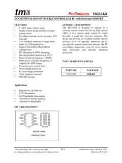
3 Green Device (Note 3) Pin Assignments (Top View) 12348765 SWCSFBCOMPNCVCCVINNCEP SO-8EP Applications Non-dimmable MR16 Lamps Dimmable MR16 Lamps General Illumination Lamps Notes: 1. No purposely added lead. Fully EU Directive 2002/95/EC (RoHS) & 2011/65/EU (RoHS 2) compliant. 2. See for more information about Diodes Incorporated s definitions of Halogen- and Antimony-free, "Green" and Lead-free. 3. Halogen- and Antimony-free "Green products are defined as those which contain <900ppm bromine, <900ppm chlorine (<1500ppm total Br + Cl) and <1000ppm antimony compounds.
4 Typical Applications Circuit D2D1D3D4D5 RSETRHYSCOC3 SWCSVCCCOMPVIN(Exposed Pad)LC4 VacAL8821 FBRFB AL8821 Document number: DS37671 Rev. 2 - 2 2 of 14 February 2017 Diodes Incorporated AL8821 NEW PRODUCT Pin Descriptions Pin Number Pin Name Function 1 SW Integrated MOS Drain 2 CS Input current Sense Pin 3 FB LED Output current Feedback Pin 4 COMP Control Loop Compensation Pin 5 NC Not Connected 6 VIN IC Input Voltage, Adding from BOOST Output Voltage 7 VCC Supply Voltage For Internal Circuit 8 NC Not Connected 9 Exposed Pad Connected to Ground Functional Block Diagram VINUVLOChip_ENVBGE xposed PadEAFBVBGCOMPCS1 CSVCS1 SWCOMPARATOROVPVFBOVPOTPOTPB andgapVBGVCCVREFLOGICD riverVCCI nternal RegulatorVCCVINIHYSIHYSPWM1 PWM12367149 AL8821 Document number: DS37671 Rev.
5 2 - 2 3 of 14 February 2017 Diodes Incorporated AL8821 NEW PRODUCT Absolute Maximum Ratings (@TA = +25 C, unless otherwise specified. Note 4) Symbol Parameter Rating Unit VIN VIN Pin Voltage to 40 V VSW SW Pin Voltage to 50 V VCOMP COMP Pin Voltage to 6 V VCS CS Pin Voltage to 6 V VFB FB Pin Voltage to 6 V VCC VCC Pin Voltage to 6 V TJ Operating Junction Temperature +150 C TSTG Storage Temperature -65 to +150 C JA Thermal Resistance (Junction to Ambient) (Note 5) 66 C/W TLEAD Lead Temperature (Soldering, 10sec) +300 C ESD (Machine Model) 200 V ESD (Human Body Model) 2000 V Notes: 4.
6 Stresses greater than those listed under Absolute Maximum Ratings may cause permanent damage to the device. These are stress ratings only and functional operation of the device at these or any other conditions beyond those indicated under Recommended Operating Conditions is not implied. Exposure to Absolute Maximum Ratings for extended periods may affect device reliability. 5. Device mounted on FR-4 PCB (51mm x 51mm) 2oz copper, minimum recommended pad layout on top layer and thermal vias to bottom layer ground plane. For better thermal performance, larger copper pad for heat-sink is needed.
7 Recommended Operating Conditions Symbol Parameter Min Max Unit VIN VIN Pin Voltage 5 36 V TA Ambient Temperature -40 +105 C Electrical Characteristics (@TA = +25 C, unless otherwise specified.) Symbol Parameters Conditions Min Typ Max Unit Input Supply VIN VIN Pin Voltage 5 36 V IQ Quiescent current No Switching 1 mA VUVLO Under-Voltage Lockout Voltage VIN Rising V VHYS UVLO Hysteresis 500 mV VCC Regulator VCC VCC Pin Voltage 5 V Source current Capability VCC = 5V 10 mA Load Regulation 4 % AL8821 Document number: DS37671 Rev.
8 2 - 2 4 of 14 February 2017 Diodes Incorporated AL8821 NEW PRODUCT Electrical Characteristics (Cont. @TA = +25 C, unless otherwise specified.) Symbol Parameters Conditions Min Typ Max Unit Integrated NMOS_BOOST VDS MOS Voltage Stress (Note 6) 50 V IDS MOS current Stress (Note 6) 2 A RDSON MOS RDSON 250 m Compensation and Soft Start (COMP Pin) GEA Error Amplifier Trans-conductance 1000 A/V IO-H Sourcing current VCOMP = 68 A IO-L Sinking current VCOMP = 68 A VFB FB Pin Voltage 444 mV Hysteresis Competitor VCS_MIN BOOST Sense Voltage Low Level VCOMP = 0V -90 mV IHYS Hysteresis current 85 100 115 A Over-Temperature Protection TOTSD Thermal Shutdown (Note 6) +160 C THYS Thermal Shutdown Hysteresis (Note 6) +40 C Note 6: These parameters, although guaranteed by design, are not 100% tested in production.
9 AL8821 Document number: DS37671 Rev. 2 - 2 5 of 14 February 2017 Diodes Incorporated AL8821 NEW PRODUCT Performance Characteristics Quiescent current vs. VIN Pin Voltage Quiescent current vs. Ambient Temperature VCC Pin Voltage vs. VIN Pin Voltage VCC Pin Voltage vs. Ambient Temperature FB Pin Voltage Pin Voltage FB Pin Voltage vs.
10 Ambient Temperature Quiescent current (mA)VIN Pin Voltage (V) Quiescent current (mA)Ambient Temperature (oC)VIN = VCC Pin Voltage (V)VIN Pin Voltage (V) VCC Pin Voltage (V)Ambient Temperature (oC)VIN = FB Pin Voltage (V)VIN Pin Voltage (V) FB Pin Voltage (V)Ambient Temperature (oC)VIN = 12V AL8821 Document number: DS37671 Rev. 2 - 2 6 of 14 February 2017 Diodes Incorporated AL8821 NEW PRODUCT Performance Characteristics (Cont.) BOOST Sense Voltage Low Level vs. BOOST Sense Voltage Low Level vs.