Transcription of Build a Class-A Amplifier - FIRST WATT
1 Build a Class-A AmplifierAudio Feb, 1977 by Nelson PassIn spite of their high cost and low efficiency, class A power amplifiers have recently beenreceiving more attention from audiophiles who demand uncompromising accuracy. Boththe price and quality of these amplifiers result from the operation of their output stages inclass A mode, where the amplifying devices are constantly operated in their linear region,above cutoff and below saturation. Whether made from tubes or semiconductors, circuitsoperating in class A mode yield the smoothest transfer functions and widest bandwidths,hence their near universal application in preamplifiers and other low power audio power amplifiers use class A circuitry exceptin the drive and output stages, where they use class B orAB operating modes to achieve high efficiency. In classB and AB modes, the output stage operates in a push-pull configuration, where one set of output devicesdelivers positive voltage and current and another setdelivers negative voltage and current.
2 When one set isworking, the other set is turned off. This schemeoperates efficiently, but has two serious flaws, theextremely nonlinear characteristic of the transistors atthe collector cutoff region and the turn-on/turn-off times of the devices. Designers oftransistor amplifiers have tended to use large amounts of negative feedback to correct forthe nonlinearities, but this works well only at low frequencies. At high frequencies, thefeedback loop is unable to make adequate corrections, and the distortion that occurs at theoutput is aggravated by overloaded front-end usual total harmonic and intermodulationdistortion figures do not reveal the abrupt output stagedistortions accurately because of the averaging factorinvolved in such measurements. A spike of crossoverdistortion may reach 2 per cent, but if it occurs onlyover 5 per cent of the waveform, it averages out to arespectable per cent distortion figure.
3 Consideringthis error factor, it is easy to see why two amplifierswith the same specifications can sound so different. Toproperly evaluate the distortion, peak distortion andharmonic distribution must be considered. Typical class A amplifiers will exhibit loworder harmonics, and their peak distortion is less than twice the average distortion. Inclass AB amplifiers, very high orders of harmonics occur, and the peak distortion can beas much as thirty times the average problem common to class B and AB output stages is due to the unequal turn-on/turn-off times of the transistors. Because the turn-off time is greater, both transistorsets can conduct uncontrollably under high slew conditions, making it dangerous tooperate the Amplifier at high frequencies, a particularly bad problem with some quasi-complementary a class A output stage, however, there are no abrupt nonlinearities and no turn-on/turn-off delays.
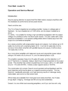
4 The smooth transfer characteristic yields low order harmonic distortions, andthese harmonics can easily become unmeasurable at low power the course of our research, we developed a small class A power Amplifier whichdelivers 20 watts into 8 ohms. It offers excellent performance over a wide bandwidth, andthe design is simple and stable enough that it can be built by the advanced constructor atlow cost and with a minimum of test equipment. The parts utilized are usually availableoff the shelf from Motorola and RCA distributors, and the design will accommodate theusual variations in components without problems, so that it is unnecessary to selectsemiconductors for particular characteristics. A stereo version of this Amplifier can bebuilt for approximately $ basic circuit configuration is shown in Fig. 1, where an input differential transistorpair drives a current-sourced transistor, forming the two voltage-gain stages of theamplifier.
5 The output of the second voltage-gain transistor drives a triple emitter-followeroutput stage, which provides a current gain of somewhat less than a million. The fourcurrent sources in the circuit are used to simultaneously increase the bandwidth andlinearity, accomplishing this by idling semiconductors at currents much larger than thecurrents required to drive the Amplifier . With the exception of the output stage, the gaintransistors operate with only small variations about their operating compensation capacitor shown in Fig. 1 is used to provide damping for the circuit,eliminating overshoot and ringing in the output. Its effect is the reverse of the usual lagcompensation employed in transistor amplifiers because it actually reduces transientintermodulation effects by creating an internal high frequency feedback loop similar tothe damping circuits found in servo systems, where the front end of the Amplifier cansatisfy its own loop requirements at high frequencies, avoiding front-end schematic of the actual Amplifier is presented in Fig.
6 2. The transistorsQ3,6,7,13,14,15,16 form the current sources of Fig. 1. Their current value is governed bythe active voltage source of Q8, where the circuit is stabilized by taking feedback fromR22. This current sourcing system accurately tracks the current value once it is properlyadjusted. The one-toone circuit board pattern and an upsized parts location guide aregiven in Fig. 3 and Fig. 4. The location of the parts is self explanatory, except that Q5 andQ7 must be fitted with heat sinks. Reasonable care must be taken to avoid overheating thesemiconductors and other components during soldering, and high-wattage soldering gunsmust not be used. If any substitute transistors are used, it may be necessary to adjust thevalues of C7 and C4 for stable operation using an 8-ohm non-inductive load and drivingthe Amplifier with 100 kHz square waves. If the Amplifier should exhibit high frequencyoscillation, increase the value of C4 or decrease the value of this Amplifier , there is no such thing as too much heat sinking for the output in this area is no vice, and good ventilation is similarly very important.
7 Theuse of more than 100 square inches of black-anodized aluminum heat sink per outputtransistor should allow for operation without a fan. A safe rule of thumb by which toevaluate the quality of heat sinking is to see whether or not you can place your hand onthe heat sink without hurting yourself. The heat sink should be grounded to the chassis ofthe Amplifier , and heat-conducting insulators must be used with a liberal quantity ofsilicone grease between the heat sink and the output 5 shows the power supply for a two-channel system which will allow differentsupply voltages for optimization of the output power versus load impedance. The 105volt primary tap of the transformer will serve for 8-ohm loads, the 115 volt tap for 6-ohmloads, and the 125 volt tap for 4-ohm loads. With a 120 volt line, the maximumpower yield is 20 watts per channel into 8 ohms, 24 watts into 6 ohms, and 28 watts into4 ohms.
8 To alter the Amplifier for optimal performance into a given load, the tap must bechanged and the Amplifier must be rebiased. If the diode bridges in the power supply arenot mounted on a metal chassis, they too must be provided with heat sinks. Use 16-gaugewiring in the power supply and Amplifier output connections, while 24-gauge wire isadequate for other connections. It is important that all of the ground connections beshared by both channels at one point on the ground bus. The ground bus must connect allfour power supply capacitors and be of heavy gauge. Additional wiring information isgiven in Fig. 6, where the grounding and power connections are to be followed literallyfor low noise. At the input connectors, the ground of the input is physically isolated fromthe chassis. A uF capacitor connects each input ground to the chassis at the input andis used to eliminate UpBiasing the Amplifier is quite easy with either a voltmeter or an oscilloscope.
9 Beforeturning on the Amplifier , R16 must be adjusted for maximurn resistance (minimum biascurrent). If the bias is set too high, the negative power supply fuse will blow withoutdamaging the circuit. If this occurs at one extreme setting of the potentiometer, replacethe fuse, set the pot to the other extreme, and try again. After the Amplifier is turned onand doesn't blow the fuses, the bias must be set by adjusting R16, preferably using anoscilloscope. Using an oscilloscope, the bias is adjusted by driving the Amplifier with asine wave into the appropriate load resistor value. Set R16 so that the Amplifier clips intothe load on the negative half of the wave before the positive half clips. Then operate theamplifier for 15 minutes without an input signal. After 15 minutes, readjust the bias forsymmetrical clipping of the circuit when it is very slightly overdriven.
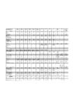
10 Repeat theadjustment again in 15 minutes to insure that the heat sinks have reached using a high quality voltmeter, the bias can be adjusted by a similar procedure,measuring the voltage occuring across R22. For an 8-ohm load, the voltage across R22should be 125 millivolts. For 6 ohms, the voltage is to be 170 mV, and 220 mV for 4-ohm loads. As before, the bias must be adjusted slightly low and increased slowly to theproper value after the Amplifier has warmed up. The voltage should be monitored andadjusted periodically over a half an hour or prototype Amplifier was built without specially selected components and the onlyadjustments made were the output bias currents. The Amplifier yielded the performancefigures shown in Table Amplifier 's response to square waves is shown at 20 Hertz (Fig. 7) and at 100,000 Hertz (Fig. 8). Figure 9 shows the waveform at 500,000 Hertz at 6 dB power level.