Transcription of Sony VFETs in Push-Pull Class A - FIRST WATT
1 sony VFETs in Push-Pull Class APart 2: Common Drain Modeby Nelson PassThis article is the second of a series presenting Do-It-Yourself audio power amplifiers using Static Induction Transistors (SITs), also known as VFETs . These are unusual transistors with a characteristic similarity to Triode than recapitulate much of what I have already written about these devices, I refer you to previous articles linked below. I recommend looking at these for background SIT Introduction 2012 SIT Nemesis 2013 sony VFET 40 Year Commemorative Amplifier 2014 sony VFETs Part 1 2011 SIT-1 Owner's Manual 2011 SIT-2 Owner's Manual The most recent of these, Part 1, is a simple DIY amplifier having just three components two transistors and a transformer.
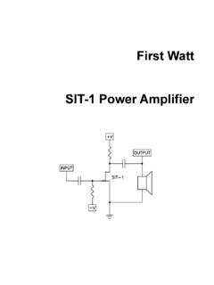
2 It is very simple to build, although it requires four regulated power supplies. It operates in Common-Source mode, in which the gain transistors develop both voltage and current gain. Part 2 shows VFETs operating in Common-Drain, or follower amplifier is more complex than Part 1, and has many more components. It can be regarded as the smaller brother of the sony 40 Year Commemorative Amp with fewer parts and less power, however we will be adding a couple of interesting wrinkles, including local Cascode feedback, operation with and without global feedback, and also a modulated supply regulation is designed as a DIY project, and as of this writing you can still obtain the VFETs from in Singapore, but probably not for too much is a simplified diagram of the circuit:If you have absorbed the contents of the previous articles, you probably have a good picture of what is going on.
3 To make it a little easier, I have identified the generic part types, and also the pin names: Drain, Source and Gate. You can see the input and output points, and also the two voltage sources used create the DC Gate voltages that set the output transistors to the desired bias current. When we talk about bias we are referring to the voltage and/or current that set the operating point from which they can amplify without a lot of distortion. Proper bias conditions are crucial to low from the left, the input drives the Gates of a complementary pair of JFET signal transistors in Common Source mode.
4 These two devices are depletion type Fets which will self-bias to a current of 8 milliamps or current through the input Fets develops voltage at their Drains to create the signals that drive the second stage, which is a complementary pair of MOSFETs in Common-Source mode also, with their Drains tied together at a point where the entire voltage gain of the amplifier can be seen. This point drives the Gate pins of complementary VFETs in Common-Drain (follower) mode, and they provide the current gain which drives the output bias circuits supply negative DC voltage to the N type VFETs and positive to the P types.
5 VFETs are also depletion mode parts, where current likes to flow with 0 volts input, and the bias circuit is like using a brake pedal. Most MOSFET parts are enhancement mode parts, and have to be encouraged to conduct; the bias circuit in their case is more like an accelerator the transistors involved were more perfect, then we could just stop there. But of course they are not, and as with most other amplifiers, lots of circuitry is employed trying to overcome the flaws of the gain is a slightly more complex version of the circuit:On the left side, the voltage gain stage, we can see new elements.
6 We have degenerating resistors in series with the Source pins of the MOSFETS to lower the gain and stabilize the bias current against temperature drift. We have also introduced Cascode transistors for the input JFET devices and biased them with some constant voltage sources, and we have also introduced local Cascode feedback to linearize the gain and lower the output impedance of the front is a very useful technique which shields the gain devices from the consequences of the voltages that appear on their Drain pins. In this case it limits the Drain-Source DC voltage seen by the JFETs and their heat dissipation, and also reduces the gain modulation caused by AC and DC variations seen by the input can read more about Cascoding here: 1978 Cascode Amplifiers Cascoding also gives us a simple means of applying local feedback to the second stage by providing a convenient summing junction from the Drains of the MOSFETs to the Emitters of the Cascode transistors.
7 I named this Cascode feedback , and FIRST employed it in the Xs amplifiers from Pass is most useful for applying modest amounts of local Drain-Gate feedback without degrading the power supply rejection (PSRR) of the stage. This is a simple case, where the front end starts out with a gain of about 26 dB, and after the application of Cascode feedback we see get 16 dB, for a feedback factor of about 10 dB. Being modest and very local, it is also very stable. There are numerous variations and lots of little tricks, and besides lowering the output impedance of the front end, it is convenient and effective for reducing and tweaking the specific distortion character of the circuit, as the positive and negative halves of the circuit can be adjusted far we have only seen arrangements where all the feedback (such as it is) is local to individual elements of the amplifier, mostly the ratios of the various resistors in the front end.
8 Later we will see arrangements for global the right hand side of the drawing we will see more details about the output stage. More specific bias circuitry shows that the bias voltage is actually referenced to ground, and the Gates of the VFETs are coupled to the voltage gain stage through parallel RC more interest, the output stage has acquired power voltage regulators, which keep the voltage seen on the Drains of the VFETs at known quiet DC value. The reason for this is simple; the VFETs have a low Drain impedance. That means that any power supply variation or noise will go through the Drain to Source channel to the output.
9 We don't need any of that, and if we had it we would be forced to employ negative feedback to correct power supply regulators are simply constant voltage sources driving big power Mosfets as followers. Very simple, works like , gird your grid for the big one:If this looks intimidating, remember that its simply a detailed look at the sub-circuits we have seen already, each of them relatively 's look at them individually:The input transistors Q11 and Q12 are the Toshiba JFETs 2SK170 and 2SJ74, no longer made, but can be substituted by LSK/LSJ versions from Linear Systems without problems.
10 These are matched for Idss values of about 8 mA, Idss being the current that flows when the Gate and Source voltage are equal. The Sources of the input devices do not have degenerative resistance between each other, so they will run at this input Gates look at the signal through a resistor, which provides some input radio frequency filtering when loaded by the input capacitance of the JFETs, and also some protection from high voltage input current through the JFETs and the Bipolar Cascode transistors develops about 4 volts across R43 + P3 on the positive side, and R44 + P4 on the negative side.