Transcription of Chapter 8:Field Effect Transistors (FET’s)
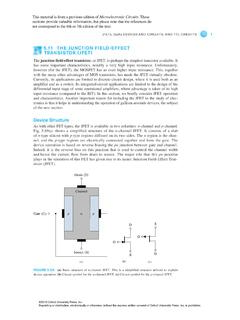
1 1 Chapter 8:Field Effect Transistors (FET s) The FET The idea for a field- Effect transistor (FET) was first proposed by Julius Lilienthal, a physicist and inventor. In 1930 he was granted a patent for the device. His ideas were later refined and developed into the FET. Materials were not available at the time to build his device. A practical FET was not constructed until the 1950 s. Today FETs are the most widely used components in integrated circuits. 28-1: The Junction Field Effect Transistor (JFET) The JFET ( junction field- Effect transistor) is a type of FET that operates with a reverse-biased pnjunction to control current in a channel. JFETs has two categories, n channel or p channel. For n-channel JFET shown; the drain (D) is at the upper end, and the source (D) is at the lower end. Two p-type regions are diffused in the n-type material to form a channel, and both p-type regions are connected to the gate (G) lead.
2 For p-channel, the gate is connected to n-type regions forming the channel into the p-type materialbasic structure of the two types of Structure8-1: The Junction Field Effect Transistor (JFET)Basic Operation Biasing of JFET is shown in the figure VDDprovide drain-to-source voltage current flow from drain to source VGGsets the reverse bias between the gate and the source sets the depletion region along the pn junction restricting channel width increase channel resistance38-1: The Junction Field Effect Transistor (JFET)Basic Operation By varying the gate voltage (VGG) increasing ve voltage between G and S varying the channel width controlling the amount of drain current (ID); As VGGincrease depletion region increase channel decrease higher resistance lower current Depletion region The schematic symbols for both n-channel and p-channel JFETs are shown in the adjacent figure; the arrow on the gate points in for n channel and out for p : JFET Characteristics And ParametersThe JFET operates as a voltage-controlled, constant-current device Drain characteristic curve If you set the gate-to-source voltage to be zero (VGS= 0) by shorting gate-to-source as shown as VDDincrease, IDincrease and thus VDSincrease (Ohmic regionbetween A and B constant R between D and G).
3 At point B (at VDS= pinch-off-voltage -Vp) current IDbecomes constant (active region between B and C); this is due to reverse bias voltage from gate-to-drain VGDwhich prevent any further increase in IDwith increasing VDS at point C where ID rapidly increase breakdown region JFET may damagemax. drain current for given JFET. It is usually specified at VGS= 048-2: JFET Characteristics And Parameters When VGSis set to different values, the relationship between VDSand IDdevelops a family of characteristic curves for the device (figure below). Drain characteristic curve The figure shows the more negative VGSis, the smaller ID(constant smaller current begins at pinch-off) becomes in the active region. When VGShas a sufficiently large negative value, IDis reduced to zero VGS= VGS(off) (cut off voltage).
4 This cutoff Effect is caused by the widening of the depletion region to a point where it completely closes the channel Note that pinch off is different than pinch off voltage measured when VGS= 0 Vpis positive and has the same magnitude as VGS(off).8-2: JFET Characteristics And ParametersExample:from KVLIf VDDincreases to 15 V VDSwill increase. But IDwill remain the same 58-2: JFET Characteristics And ParametersJFET Universal Transfer Characteristic Because VGS control the drain current ID a plot of the output current (ID) to the input voltage (VGS), called the transfer or transconductance curve, can be drawn:general transfer characteristic curve between VGSand ID8-2: JFET Characteristics And ParametersJFET Universal Transfer Characteristic The transfer characteristic curve can also be developed from the drain characteristic curves by plotting values of IDfor the values of VGStaken from the family of drain curves at pinch-off (at different constant drain currents).
5 For different VGS, JFET ID s can be mathematically expressed by 68-2: JFET Characteristics And ParametersExample:JFET Forward Transconductance The transconductance (transfer conductance), gm(or gfsoryfs-forward transfer admittance), is an important factor in determining the voltage gain of a FET amplifier as you will see later. gmis the ratio of a change in output current ( ID) to a change in the input voltage ( VGS): As VGSincrease resistance increase conductance decrease gmhas its highest value (gm0) at VGS= 0 as shown in the figure for given VGShas the unit of siemens (S). At given VGS, gmcan be calculated using where8-2: JFET Characteristics And Parameters7 JFET Forward Transconductance: Example:for a 2N5457 JFET: typically, IDSS= mA, VGS(off)= -6V maximum, and gfs(max)= 5000 mS. Using these values, determine the forward transconductance for VGS= -4V, and find IDat this : JFET Characteristics And ParametersInput Resistance and Capacitance Input resistance (RIN) of the JFET is the resistance of the reverse-biased gate-source junction At given VGSwith reverse gate-source current IGSS The input capacitance, Ciss, is a result of the JFET operating with a reverse-biased (depletion layer act as a capacitor in reverse biase)See Example 8-5AC Drain-to-Source Resistance For JFET, RINis usually very high and decrease with temperature, T, since IGSS increases with T.
6 Above the pinch off, IDis relatively constant; Only small change in IDoccurs over a wide range of VDS we have ac drain-to-source resistance Datasheets specify this parameter as output conductance, gos, or output admittance, yos, for VGS= 0 : JFET Characteristics And Parameters88-3: JFET BiasingWe can use the JFET parameters discussed to properly bias the JFET by dc voltage (VGS) and determine a proper Q-point. Three types of bias are self-bias, voltage-divider bias, and current-source - Self-Bias Self-bias is simple and effective, so it is the most common biasing method for JFETs. With self bias, the gate is essentially at 0 V. For n-channel, RSis added to makes the source positive with respect to ground (ISproduce a voltage drop across RS) RSdevelops the necessary reverse bias that forces the gate voltage (VG = 0; IG=0) to be less than the source.
7 The inverse is for p-channel JFET must be operated such that the gate-source junction is always reverse-biased. -veVGSfor an n-channel JFET and a +veVGSfor a p-channel JFET. This can be achieved using the self-bias arrangements shown8-3: JFET Biasinga - Self-Bias: Setting the Q-point The gate to source voltage isSince IS= IG + ID = 0 + ID = IDDGSSIVR= Which can be found for certain Q-point (certain VGSand ID) as shown for the given transconductance the shown curve, the value of RSto self bias JFET at VGS= -5V isReverse current; ideally = 098-3: JFET Biasinga - Self-Bias: Setting the Q-point It is usually preferable to bias the JFET near the mid point of it s transfer curve (at ID= IDSS/2 and VD= VDD/2) midpoint bias allows the maximum amount of drain current swing between IDSSand 0 when there is an ac signal applied to and substitute for ID = IDSS/2 VGS= VGS(off) (off)To set the drain voltage at midpoint (VD= VDD/2), select a value of RDto produce the desired voltage : JFET Biasinga - Self-Bias: Setting the Q-point: Exampleselect resistor values for RDand RSin Figure to set up an approximate midpoint bias.
8 108-3: JFET Biasinga - Self-Bias: Setting the Q-point Indeed, for a given circuit, you can use the transfer curve of a JFET and certain parameters to determine the Q-point (IDand VGS) of a self-biased circuit. For shown circuit with shown transfer curve, the Q-point can be determined by:a) Draw the transfer curveb) calculate VGSwhen IDis the first point ID=0 and VGS= 0 - origin point(c) calculate VGSwhen ID= IDSSS etting the second point ID= IDSSand VGS= -IDRS(d) Connect between the two points on the curve by a line (dc load line) the intercept of the line with transfer curve is the Q-point stability of Q-point can be increased by increasing RSand connect it to a negative bias voltage dual supply bias8-3: JFET Biasingb - Voltage-Divider Bias and the Q-pointVoltage-divider biasing shown is a combination of a voltage-divider and a source resistor to keep the source more positive than the gate gate-source junction is reverse biased.
9 The dc voltages (determining the Q-point) can be found by as followed:and by voltage divider, gate voltage is Source voltage isThe gate-source voltage then isThe drain current Note that ID= ISorDrain current can also be calculated if you know VD 118-3: JFET Biasingb - Voltage-Divider Bias: Example In this example, If VDhad not been given, the Q-point values could not have been found without the transfer characteristic : JFET Biasingb - Voltage-Divider Bias and the Q-point Q-point can also be graphically determine the Q-point of a circuit on the transfer characteristic curve as followed: a) Draw the transfer curveb) calculate VGSwhen IDis the first point ID= 0 and VGS= VGc) For VGS= 0 Setting the second point VGS= 0 and ID= VG/RS(d) Draw the voltage divider dc load line between the two points the intercept of the line with transfer curve is the Q-point 128-3: JFET Biasingc Current Source Bias stability of Q-point Unfortunately, the transfer characteristic of a JFET can differ very much from one device to another of the same type.
10 For example for two devices of 2N5459 JFET, you may have two different IDSSand VGS(off)as shown on self biase transfere curve the Q-point could be any value between the minimum Q1and maximum Q2 not fixed IDand VGSfor given device number since ID is not stable means the Q-point is not : JFET Biasingc Current Source Bias stability of Q-point Indeed, stability of Q-point in self biased JFET can be increased by providing a given constant IDthrough adding a constant current source in series with JFET as shown The current-source can be either a BJT or another FET. With current-source biasing, the drain current, ID, is constant IEand is essentially independent of current sourcebutThe emitter current138-3: JFET Biasingc Current Source Bias stability of Q-point Also the Q-point in voltage divider bias for devices of same type is consider to be more stable because the slope of voltage divider dc load line is less than that in self bias JFET as shown.