Example: barber
Lecture 25: CS, CD and CG circuits
For about a week, we will continue with chapter 8 in the text, single stage amplifiers. We will focus primarily on FET circuits, Common Source(CS) , Common Gate (CG), and Common Drain(CD), sections: 8.1,8.3, 8.4, 8.5, 8.8, 8.9 Following single transistor configurations, we will start discussing multistage and cascaded circuits,
Tags:
Information
Domain:
Source:
Link to this page:
Documents from same domain
Diodes and Transistors
inst.eecs.berkeley.eduDiodes and Transistors 1. ... basic semiconductor physics. We won’t discuss the details because the point of this ... switch. Below the specified ...
HSPICE Tutorial - University of California, Berkeley
inst.eecs.berkeley.eduHSPICE Tutorial Contents 1 Introduction 1 ... ee105 spice tutorial example 1 - simple rc circuit in the Results Browser and double-clicking vs and vo to plot them in the graph. You may have been able to guess from the netlist, but you’ll see that vsis a …
Introduction to LabVIEW - University of California, …
inst.eecs.berkeley.eduIntroduction to LabVIEW 1. Introduction Welcome to the LabVIEW component of EE100! This lab is just a simple introduction to the graphical circuit simulation ...
Introduction to LabVIEW For Use in Embedded …
inst.eecs.berkeley.eduUC Berkeley EE249 Hugo.Andrade@ni.com Introduction to LabVIEW For Use in Embedded System Development
EE105 –Fall 2015 Microelectronic Devices and Circuits
inst.eecs.berkeley.eduSummary of MOS Single-Transistor Amplifiers MOS Common Source Common Source with Deg. Common Drain Common Gate Ri ∞ ∞ ∞ Small Ro Large Very Large Small Large
Introduction to Digital Systems - University of …
inst.eecs.berkeley.eduDepartment of EECS EE100/42-43 Spring 2007 Rev. 1 Introduction to Digital Systems 0. Acknowledgments Many thanks to Prof. Bernhard Boser and National Instruments for funding this project in the
EE126: Probability and Random Processes - Lecture 1 ...
inst.eecs.berkeley.eduprobability 4 The probabilities summed over all of the base outcomes always equals 1 Example: Toss a fair coin twice 1 Base outcomes are HH,HT,TH,TT 2 This covers all the possibilities. M.E. 3 Each of these outcomes is equally likely 4 Assign each outcome a probability of 0:25. The list (set) of base outcomes is called the Sample Space.
EECS 126 Probability and Random Processes: Course Syllabus ...
inst.eecs.berkeley.eduDescription: Probability is a mathematical discipline that allows one to reason about uncertainty: it helps us to predict uncertain events, to make better decisions under uncertainty, and to design and build systems. Throughout the course, we will teach you the fundamental ideas of probability and random processes along with the labs.
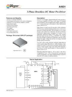
3-Phase Brushless DC Motor Pre-Driver
inst.eecs.berkeley.eduDescription The A4931 is a complete 3-phase brushless DC motor pre-driver . The device is capable of driving a wide range of N-channel power MOSFETs and can support motor supply voltages up to
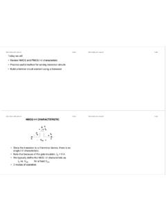
DS -V I G - EECS Instructional Support Group Home Page
inst.eecs.berkeley.eduG D S I D I G-V DS + + V G S _ NMOS I-V CHARACTERISTIC • Since the transistor is a 3-terminal device, there is no single I-V characteristic. • Note that because of the gate insulator, I G = 0 A. • We typically define the MOS I-V characteristic as I D vs. V DS for a fixed V GS. • 3 modes of operation
Related documents

Audio Power Amplifier - de Smith
www.desmith.netChapter 6 The output stage II Distortion number 4: VAS loading distortion ... The biasing requirements The linearity issues of series Class-G The static linearity ... Chapter 12 FET output stages The characteristics of power FETS FET versus BJT output stages Advantages of FETs
Chapter 6 FET Biasing - Khon Kaen University
home.kku.ac.thChapter 6 FET Biasing Chapter 6 FET Biasing 1 INTRODUCTION The general relationships that can be applied to the dc analysis of all FET amplifiers are and For JFETs and depletion-type MOSFETs, Shockley’s equation is applied to relate the input and output quantities: For enhancement-type MOSFETs, the following equation is applicable:
The Art of Electronics
artofelectronics.net2.6 Some typical transistor circuits 123 2.6.1 Regulated power supply 123 2.6.2 Temperature controller 123 2.6.3 Simple logic with transistors and diodes 123 Additional Exercises for Chapter 2 124 Review of Chapter 2 126 THREE: Field-Effect Transistors 131 3.1 Introduction 131 3.1.1 FET characteristics 131 3.1.2 FET types 134
CRYSTAL OSCILLATOR CIRCUITS
bgaudioclub.org7.6. Butler Harmonic Circuits, C-tap89 7.7. Butler Harmonic Circuits, L-tap93 6. TRIMMING THE CRYSTAL FREQUENCY101 9. THE START-UP PROBLEM 103 9.1. Biasing ICs 103 9.2. Biasing Discrete Transistors 105 10. DISCRETE TRANSISTOR OSCILLATORS 109 A. Circuit Selection and Testing109 B. Fundamental Circuits 111 10.1. Miller-FET 111 10.2. Miller ...
Lecture 17: Clock Recovery - Stanford University
web.stanford.edu• FET’s are non-linear but what we really need is to clamp the swing. Also if load transfer function is symmetric CMRR is improved [19] • Use replica feedback biasing to cancel substrate and supply noise Sum of transistor I-V and diode-connected I-V curve Ids Vds Vctrl @ various V ctrl Vbias Vctrl i+ i-o- o+-+ Replica loop k eeps the s wing

II PU Midterm Exam Syllabus November 2021
www.jaincollege.ac.in2. Bipolar Junction Transistor (BJT) Biasing 3. Transistor Amplifiers 4. 10. Digital Electronics TERM – II [ Analog Electronics] 1. Field Effect Transistor (FET) Feedback in Amplifiers 5. Operational amplifier (Op-Amp) 6. Oscillators FRENCH 1.Tenses (présent, futur proche, passe récent, passe compose, imparfait, future simple, présent ...
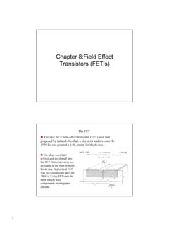
Chapter 8:Field Effect Transistors (FET’s)
staff-old.najah.edu2 8-1: The Junction Field Effect Transistor (JFET) The JFET ( junction field-effect transistor) is a type of FET that operates with a reverse-biased pn junction to control current in a channel. JFETs has two categories, n channel or p channel. For n-channel JFET shown; the drain (D) is at the upper end, and the source (D) is at the lower end. Two p-type regions are diffused in
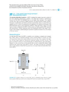
5.11 THE JUNCTION FIELD-EFFECT TRANSISTOR (JFET)
global.oup.comAs with other FET types, the JFET is available in two polarities: n-channel and p-channel. Fig. 5.69(a) shows a simplified structure of the n-channel JFET. It consists of a slab of n-type silicon with p-type regions diffused on its two sides. The n region is the chan-nel, and the p-type regions are electrically connected together and form the ...

7. Low-Noise Amplifier Design - Cambridge University Press
www.cambridge.org6 Design philosophy Take advantage of what silicon does best: transistors. Use Si passives only sparingly: Q is fairly low and undermines overall noise figure Inductors are (significantly) larger than transistors, hence expensive. Make transistor sizing part of the noise matching step. Use only reactive (loss-less) feedback or minimize the