Transcription of 3-Phase Brushless DC Motor Pre-Driver
1 DescriptionThe A4931 is a complete 3-Phase Brushless DC Motor Pre-Driver . The device is capable of driving a wide range of N-channel power MOSFETs and can support Motor supply voltages up to 30 V. Commutation logic is determined by three Hall-element inputs spaced at 120 .Other features include fixed off-time pulse width modulation (PWM) current control for limiting inrush current, locked-rotor protection with adjustable delay, thermal shutdown, overvoltage monitor, and synchronous rectification. Internal synchronous rectification reduces power dissipation by turning on the appropriate MOSFETs during current decay, thus shorting the body diode with the low RDS(on) MOSFET. Overvoltage protection disables synchronous rectification when the Motor pumps the supply voltage beyond the overvoltage threshold during current A4931 offers enable, direction, and brake inputs that can control current using either phase or enable chopping. Logic outputs FG1 and FG2 can be used to accurately measure Motor rotation.
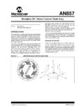
2 Output signals toggle state during Hall transitions, providing an accurate speed output to a microcontroller or speed control temperature range is 20 C to 105 C. The A4931 is supplied in a 5 mm 5 mm, 28-terminal QFN package with exposed thermal pad. This small footprint package is lead (Pb) free with 100% matte tin leadframe , Rev. 6 Features and Benefits Drives 6 N-channel MOSFETs Synchronous rectification for low power dissipation Internal UVLO and thermal shutdown circuitry Hall element inputs PWM current limiting Dead time protection FG outputs Standby mode Lock detect protection Overvoltage protection3-Phase Brushless DC Motor Pre-DriverPackage: 28-contact QFN (ET package)Typical ApplicationA4931 Approximate Scale 1 F2 k VINVINFG1 SystemControlLogicFG2A4931 HBIASDIRGNDBRAKEZENABLECP1 CLDCP2 VCPGLASAGHAGLBSBGHBGLCSCGHCSENSEHA+ HA HB+ HB HC+ HC 3-Phase Brushless DC Motor Pre-DriverA49312 Allegro MicroSystems, LLC115 Northeast CutoffWorcester, Massachusetts 01615-0036.
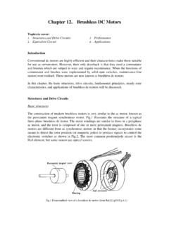
3 Maximum RatingsCharacteristicSymbolNotesRatingUn itsLoad Supply VoltageVBB38 VMotor Phase OutputSXtw < 500 ns 3 VHall InputVHxDC to 7 VLogic Input Voltage RangeVIN to 7 VOperating Ambient TemperatureTARange M 20 to 105 CMaximum Junction TemperatureTJ(max)150 CStorage TemperatureTstg 40 to 150 CSelection GuidePart NumberPackingPackageA4931 METTR-T1500 pieces per reel5 mm x 5 mm, mm nominal height QFNT hermal Characteristics CharacteristicSymbolTest Conditions*RatingUnitsPackage Thermal Resistance, Junction to AmbientR JA4-layer PCB based on JEDEC standard32 C/WPackage Thermal Resistance, Junction to Exposed PadR JP2 C/W*For additional information, refer to the Allegro Brushless DC Motor Pre-DriverA49313 Allegro MicroSystems, LLC115 Northeast CutoffWorcester, Massachusetts 01615-0036 ; PUMPGATEDRIVEVCPHALLC ommun-icationLogicDIRHB+HB-HALLHC+HC-HA+ HA-HALLBRAKEZENABLESENSEGLAGHAVBBVCPCP1C P2 Control LogicHBIASGNDVINS ystem LogicVINSAGHBSBGLBGHCSCGLCFG1FG2200 F2 k EnableFunctional Block DiagramNumberNameDescription1HA+Hall input A2HA - Hall input A3HB+Hall input B4HB -Hall input B5HC+Hall input C6HC-Hall input C7 GNDG round8 HBIASHall bias power supply output9CP1 Charge pump capacitor terminal10CP2 Charge pump capacitor terminal11 VBBS upply voltage 12 VCPR eservoir capacitor terminal13 SENSES ense resistor connection14 GLCLow side gate drive CNumberNameDescription15 GLBLow side gate drive B16 GLALow side gate drive A17 GHCHigh side gate drive C18 SCHigh side source connection C19 GHBHigh side gate drive B20 SBHigh side source connection B21 GHAHigh side gate drive A22 SAHigh side source connection A23FG1FG 1 speed control output (3 inputs)24FG2FG 2 speed control output ( A input)
4 25 CLDL ocked rotor detect timing capacitor26 DIRL ogic input Motor direction27 ENABLEL ogic input external PWM control28 BRAKEZL ogic input Motor brake (active low)Terminal List3-Phase Brushless DC Motor Pre-DriverA49314 Allegro MicroSystems, LLC115 Northeast CutoffWorcester, Massachusetts 01615-0036 ; CHARACTERISTICS* Valid at TA= 25 C, VBB = 24 V, unless noted otherwiseCharacteristicsSymbolTest Voltage RangeVBBO perating8 VBBOVVM otor Supply CurrentIBBfPWM < 30 kHz, CLOAD = 1000 pF 56mACharge pump on, outputs disabled, Standby mode mA IHBIAS 24 Current LimitIHBIASlim30 mAControl LogicLogic Input VoltageVIN(1)2 VVIN(0) Input CurrentIIN(1)VIN = 2 V 1< AIIN(0)VIN = V 1< AInput Pin Glitch RejecttGLITCHENB pin350500650nsDIR, BRAKEZ pins70010001300nsENB Standby Pulse Propagation DelaytdENBTo outputs Wake-up Delay, Standby ModetdHBIASCHBIAS = F 1525 sGate DriveHigh-Side Gate Drive OutputVGS(H)Relative to VBB, IGATE = 2 mA7 VLow-Side Gate Drive OutputVGS(L)IGATE = 2 mA7 VGate Drive Current (Sourcing)
5 IGateGH = GL = 4 V2030 mAGate Drive Pull Down ResistanceRGate102840 Dead Time tdead70010001300nsCurrent Limit Input ThresholdVREF180200220mVFixed Off-TimetOFF182537 sProtectionThermal Shutdown TemperatureTJTSD155170185 CThermal Shutdown HysteresisTJTSDhys141526 CVBB UVLO Enable ThresholdVBBUVR ising UVLO UVLOVCPUVR elative to 6 VLock Detect DurationtlockC = Overvoltage ThresholdVBBOVR ising LogicHall Input CurrentIHALLVIN = to V 101 ACommon Mode Input Input Voltage RangeVHALL60 mVp-pHall ThresholdsVthDifference between Hall inputs at transitions +10, 10 mVHall Threshold HysteresisVHYSTJ = 25 C102030mVTJ = 20 C to 125 C52040mVPulse Reject Filtertpulse 2 sFG FG Output Saturation VoltageVFG(sat)IFG = 2 mA Leakage CurrentIFGlkgVFG = 5 V 1 A*Typical data are for initial design estimations only, and assume optimum manufacturing and application conditions. Performance may vary for individual units, within the specified maximum and minimum input and output current specifications, negative current is defined as coming out of (sourcing) the specified device throughout the allowed operating temperature range are guaranteed by design and Brushless DC Motor Pre-DriverA49315 Allegro MicroSystems, LLC115 Northeast CutoffWorcester, Massachusetts 01615-0036.
6 States Table (See timing charts, below) X = Don t Care, Z = high impedanceConditionInputsResulting Pre-Driver OutputsMotor OutputHAHBHCBRAKEZENBGHA GLA GHB GLB GHC GLCABCDIR = 1 (Forward)A+ +HILOHILOLOHILOLOHILOZB+ HILOHILOLOLOLOHIHIZLOC++ HILOLOLOHILOLOHIZHILOD + HILOLOHIHILOLOLOLOHIZE + +HILOLOHILOLOHILOLOZHIF +HILOLOLOLOHIHILOZLOHIDIR = 0 (Reverse)A+ +HILOLOHIHILOLOLOLOHIZF +HILOLOLOHILOLOHIZHILOE + +HILOHILOLOLOLOHIHIZLOD + HILOHILOLOHILOLOHILOZC++ HILOLOLOLOHIHILOZLOHIB+ HILOLOHILOLOHILOLOZHIF ault*++ +HIX LOLOLOLOLOLO Z Z ZFault* HIX LOLOLOLOLOLO Z Z ZBrake*XXXLOXLOHILOHILOHILOLOLO* DIR = Don t CareABCDEFHAHBHCFG1 SASBSCDIR = 1 = FORAF EDCBHAHBHCFG1 SASBSCDIR = 0 = REV3-Phase Brushless DC Motor Pre-DriverA49316 Allegro MicroSystems, LLC115 Northeast CutoffWorcester, Massachusetts 01615-0036 ; msStandby ModeTurn off Hall Bias SupplyOutputs DisabledOutputs EnabledOutputs EnabledtdENBVBBC hargePumpVBB+ DisabledOutputs EnabledPower-up and Standby Modes Timing DiagramPower-up and Standby Modes Timing Diagram3-Phase Brushless DC Motor Pre-DriverA49317 Allegro MicroSystems, LLC115 Northeast CutoffWorcester, Massachusetts 01615-0036 ; Regulation Load current is regulated by an internal fixed off-time PWM control circuit.
7 When the outputs of the full bridge are turned on, current increases in the Motor winding until it reaches a value, ITRIP , given by:ITRIP = 200 mV / RSENSE .When ITRIP is reached, the sense comparator resets the source enable latch, turning off the source driver. At this point, load inductance causes the current to recirculate for the fixed off-time Logic The Enable input terminal (ENB pin) allows external PWM. ENB low turns on the selected sink-source pair. ENB high switches off the appropriate drivers and the load current decays. If ENB is held low, the current will rise until it reaches the level set by the internal current control circuit. Typi-cally PWM frequency is in 20 kHz to 30 kHz range. If the ENB high pulse width exceeds 3 ms, the gate outputs are disabled. The Enable logic is summarized in the following table:ENB Pin SettingOutputsOutputs State0 OnDrive 1 Source ChoppedSlow Decay with Synchronous Rectification1 for > 3 ms typicalOffDisable Fixed Off-Time The A4931 fixed off-time is set to 25 s Blank Timer When a source driver turns on, a current spike occurs due to the reverse recovery currents of the clamp diodes as well as switching transients related to distributed capacitance in the load.
8 To prevent this current spike from errone-ously resetting the source Enable latch, the sense comparator is blanked. The blanking timer runs after the off-time counter com-pletes, in order to provide the blanking function. The blanking timer is reset when ENB is chopped or DIR is changed. With external PWM control, a DIR change or an ENB on triggers the blanking function. The duration is fixed at Rectification When a PWM-off cycle is triggered, either by a chop command on ENB or by an internal fixed off-time cycle, load current recirculates. The A4931 syn-chronous rectification feature turns on the appropriate MOSFETs during the current decay, and effectively shorts out the body diodes with the low RDS(on) driver. This lowers power dissipation significantly and can eliminate the need for external Schottky Mode A logic low on the BRAKEZ pin activates Brake mode. A logic high allows normal operation. Braking turns on all three sink drivers, effectively shorting out the Motor -generated BEMF.
9 The BRAKEZ input overrides the ENB input and also the Lock Detect is important to note that the internal PWM current control cir-cuit does not limit the current when braking, because the current does not flow through the sense resistor. The maximum current can be approximated by VBEMF / RLOAD. Care should be taken to insure that the maximum ratings of the A4391 are not exceeded in the worse case braking situation, high speed and high inertial Function This function provides a power supply of V, current-limited to 30 mA. This reference voltage is used to power the logic sections of the IC and also to power the external Hall Mode To prevent excessive power dissipation due to the current draw of the external Hall elements, Standby mode turns off the HBIAS output voltage. Standby mode is triggered Functional Description3-Phase Brushless DC Motor Pre-DriverA49318 Allegro MicroSystems, LLC115 Northeast CutoffWorcester, Massachusetts 01615-0036 ; holding ENB high for longer than 3 ms.
10 Note that Brake mode overrides Standby mode, so hold the BRAKEZ pin high in order to enter Standby Pump The internal charge pump is used to generate a supply above VBB to drive the high-side MOSFETs. The volt-age on the VCP pin is internally monitored, and in case of a fault condition, the outputs of the device are Shutdown In the event of a fault due to excessive junction temperature or due to low voltage on VCP or VBB, the outputs of the device are disabled until the fault condition is removed. At power-up the UVLO circuit disables the Protection VBB is monitored to determine if a hazardous voltage is present due to the Motor generator pump-ing up the supply bus. When the voltage exceeds VBBOV , the synchronous rectification feature is Protection If die temperature exceeds approximately 170 C, the Thermal Shutdown function will dis-able the outputs until the internal temperature falls below the 15 C State Reporting The FG1 pin is an open drain output that changes state at each transition of an external Hall element.