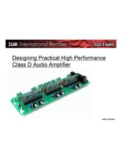
Transcription of Class D Amplifier Design Basics II - irf.com
1 Class D Amplifier Design Basics II. 02/19/2009. Rev 1. Contents Chapter 1. Getting Familiar with Class D Audio Amplifier Chapter 2. Latest Class D Audio Amplifier Technology Trend Chapter 3. Identifying Problems ~ Performance Measurement of Class D Amplifier Chapter 4. Reducing Distortion ~Dead-time ~ LPF Designs Chapter 5. Reducing Noise ~ Isolation Technique ~ PCB Design APPENDIX. Simulation of a Simple Class D Amplifier 2. Chapter 1: Getting Familiar with Class D Audio Amplifier Audio Amplifier Market Trend More Channels Smaller Box Lighter Weight A Wire with Gain More Functions (Digital Input, Diag).
2 Smaller Size Device Technology Lower Cost Control Technology Audio Performance 4. Why Class D Now? Audio Market Trend More Channels Class AB Smaller Size Smaller Size IR. Class D. Higher Performance Device Technology MOSFET. High Speed HVIC. 5. Basic Concept of Class D Audio Amplifier Class D. COMP LPF. Switching Stage Analog signal PWM Amplify PWM Analog signal VOUT = B (2D-1). In concept, Class D Amplifier is linear; 0% distortion. 6. PWM: Heart of Class D Operation Audio signal PWM PWM Audio signal 10 10. 5 5. 0 0. V. V. -5 -5. -10 -10. 60 80 100 120 140 60 80 100 120 140.
3 Time/uSecs 20uSecs/div Time/uSecs 20uSecs/div 7. Class AB vs. D Energy Point of View Similar to a variable resistor Class AB. PLOSS depends on output IIN = IOUT power factor Similar to a transformer with variable turn ratio Class D. VIN x IIN = VOUT x IOUT Bi-directional energy flow Note that input current and output current are not equal. 8. Class AB vs. D Characteristic Comparison (1/2). Feature Class D Advantage Class AB. Superior efficiency Efficiency can be improved with device technology Efficiency is fixed. Extremely inefficient when Suitable to drive lower impedance load Efficiency driving lower impedance load.
4 Can drive reactive load without significant degradation of Extremely inefficient when efficiency driving reactive load. Requires smaller power supply Bi-directional energy flow; any energy reflected from the All the reflected energy from load is recycled to the power supply. Suitable to drive reactive components and back Energy flow highly reactive load, such as woofer, speaker system EMF are consumed dissipating with dividing network, piezo speaker, etc. heat The output device has high impedance, ~tens of k ohm. Inherently has low output impedance (m ohm range) With a strong voltage feedback, Class AB can achieve low output impedance.
5 Power supply current = load Drivability current. For a given output Lower impedance loading does not burden power supply. power with decreased load (Power supply current) (load current). impedance, the supply current and heat dissipation in the output device increase. Wide power bandwidth; no extra effort to drive high Cross conduction limits high frequency rated power. frequency power bandwidth. 9. Class AB vs. D Characteristic Comparison (2/2). Feature Class D Advantage Class AB. Output device is non-linear;. exponential in BJT, quadratic in Topology is inherently linear without feedback MOSFET.
6 Strong feedback is necessary to achieve good Linearity linearity. Cross over distortion is at where load current crosses zero, Cross over distortion is not in zero crossing area which is most critical point of operation. Output devices in linear operating mode has strong Thermally stable; gain of the Class D stage, bandwidth, temperature coefficient in gain. Stability loop-gain are independent of output device temperature. Loop-gain is changing dynamically with output power. No bias-current thermal compensation Because of strong non-linearity Inherently immune to incoming noise; low drive in device and 'exposed'.
7 Noise immunity impedance, inductor between the load and Amplifier . feedback node, weak to RF. noise. Higher reliability from less heat. Less metal fatigue in Reliability solder joints. 10. Class AB vs D Comparison Loss Loss in Class AB. 2. VCC. Pc = . 8 RL. PC =. 1.. Vcc (1 K sin t ) Vcc K sin t d t 2 0 2 2 RL. Vcc 2 2K K 2 Note that this is = . 8 RL 2 independent to device parameters. K=2/ K=1. Loss Loss in Class D. Efficiency can be PTOTAL = Psw + Pcond + Pgd improved further! RDS (ON ). Pcond = Po Pgd = 2 Qg Vgs f PWM. RL. Psw = COSS VBUS f PWM K=1.
8 2. K is a ratio of Vbus and output voltage. To learn more about power losses in Class D, refer to AN-1070 Class D. Amplifier Performance Relationship to MOSFET Parameters. 11. Practical Class D Amplifier Perturbation Supply impedance Nonlinear inductance /. Limited Gain & BW Bus Pumping +VCC. Noise Figure Capacitance DC Resistance Audio PWM Gate Driver source F/B. -VCC. Dead-time Finite RDS(on). 1. Non-linearity in the switching stage due to timing errors added, such as dead-time, ton/toff, and tr/tf Vth and Qg Body diode recovery 2. Limited amount of error collection capability due Stray inductances to limited gain and bandwidth in PWM modulator 3.
9 Audio frequency band noise added in PWM RDS(ON). modulator 4. Unwanted characteristics in the switching devices, such as finite ON resistance, finite Note that of non- switching speed or body diode characteristics. ON delay OFF delay linearity corresponds 5. Parasitic components that cause ringing on to10mV out of 100V DC. transient edges bus, or in 400kHz! 6. Power supply voltage fluctuations due to its finite output impedance and reactive power flowing through the DC bus Finite dV/dt 7. Non-linearity in the output LPF. 12. MOSFET Basics A MOSFET is a device to switch In switching transition, stray electronic current.
10 A driving MOSFET impedance in each terminal slows charges/discharges a capacitor (Gate down switching and generates to Source, Gate to Drain). unwanted rings. A MOSFET does not require any energy to keep it on-state. To learn more about power MOSFETs, refer to AN-1084 Power MOSFET Basics . 13. Driving MOSFET for PWM. Only one side, either high-side or low- side, MOSFET is ON at a time. The ratio of ON time between the high- High-side ON side and low-side MOSFETs determines the output voltage. Driving a high-side MOSFET. A floating power supply that referenced to switching node drives the gate of the high-side MOSFET.