Transcription of CP2102/9 - Silicon Labs
1 Rev. 1/17 Copyright 2017 by Silicon LaboratoriesCP2102/9CP2102/9 SINGLE-CHIP USB-TO-UART BRIDGES ingle-Chip USB to UART Data Transfer- integrated USB transceiver; no external resistors required- integrated clock; no external crystal required-Internal 1024-byte programmable ROM for vendor ID, product ID, serial number, power descriptor, release number, and product description strings- EEPROM ( cp2102 )- EPROM (One-time programmable) (CP2109)-On-chip power-on reset circuit-On-chip voltage regulator- V output ( cp2102 )- V output (CP2109)-100% pin and software compatible with CP2101 USB Function controller -USB Specification compliant; full-speed (12 Mbps)-USB suspend states supported via SUSPEND pinsAsynchronous Serial Data BUS (UART)-All handshaking and modem interface signals-Data formats supported: - Data bits: 5, 6, 7, and 8- Stop bits: 1, , and 2- Parity: odd, even, mark, space, no parity-Baud rates: 300 bps to 1 Mbps-576 Byte receive buffer.
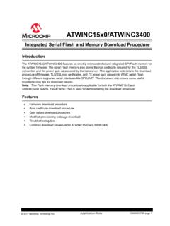
2 640 byte transmit buffer-Hardware or X-On/X-Off handshaking supported-Event character support -Line break transmissionVirtual COM Port Device Drivers-Works with existing COM port PC Applications-Royalty-free distribution license-Windows 8/7/Vista/Server 2003/XP/2000-Mac OS-X/OS-9-Linux USBX press Direct Driver Support-Royalty-Free Distribution License-Windows 7/Vista/XP/Server 2003/2000-Windows CEExample Applications-Upgrade of RS-232 legacy devices to USB-Cellular phone USB interface cable-USB interface cable-USB to RS-232 serial adapterSupply Voltage-Self-powered: to V-USB bus powered: to VPackage-RoHS-compliant 28-pin QFN (5x5 mm)Ordering Part Numbers- cp2102 -GM-CP2109-A01-GMTemperatu re Range: 40 to +85 CFigure 1. Example System DiagramCP2102 VVoltageRegulator48 MHz OscillatorINOUTSUSPENDSUSPEND1112 REGIN7 GND3 RST9D+4D-58 UARTRIDCDCTSRTSRXDTXDDSRDTR2272625242323 External RS-232 transceiver or UART circuitry(to external circuitry for USB suspend states)VBUSD-D+GND456 USB CONNECTOR61 VDDVBUSUSB FunctionControllerUSBT ransceiver640B TX Buffer576B RX Buffer1024B PROMVDDD1 D2 D3128 VPP18*CP2109 onlyFor newer designs, the CP2102N devices offer compatible footprints and are recommended for use insteadof the CP2102/9 .
3 See the Silicon Labs website ( ) for more OF CONTENTSS ectionPage1. System Overview ..42. Ordering Information ..53. Electrical Specifications ..64. Pinout and Package Definitions ..115. QFN-28 Package Specifications ..136. USB Function controller and Transceiver ..157. Asynchronous Serial Data Bus (UART) Interface ..168. Internal Programmable ROM ..179. CP2102/9 Device Drivers .. Virtual COM Port Drivers .. USBX press Drivers .. Driver Customization .. Driver Certification ..1810. Voltage Regulator ..1911. Porting Considerations from cp2102 to CP2109 .. Pin-Compatibility .. Distinguishing Factors .. Differences in Electrical Specifications .. 2212. Relevant Application Notes ..24 Document Change List ..25CP2102/94 Rev. System OverviewThe CP2102/9 is a highly- integrated USB-to-UART Bridge controller providing a simple solution for updating RS-232 designs to USB using a minimum of components and PCB space.
4 The CP2102/9 includes a USB full-speed function controller , USB transceiver, oscillator, EEPROM or EPROM, and asynchronous serial data bus(UART) with full modem control signals in a compact 5 x 5 mm QFN-28 package. No other external USBcomponents are on-chip programmable ROM may be used to customize the USB Vendor ID, Product ID, Product DescriptionString, Power Descriptor, Device Release Number, and Device Serial Number as desired for OEM programmable ROM is programmed on-board via the USB, allowing the programming step to be easilyintegrated into the product manufacturing and testing Virtual COM Port (VCP) device drivers provided by Silicon Laboratories allow a CP2102/9 -basedproduct to appear as a COM port to PC applications. The CP2102/9 UART interface implements all RS-232signals, including control and handshaking signals, so existing system firmware does not need to be modified.
5 Inmany existing RS-232 designs, all that is required to update the design from RS-232 to USB is to replace the RS-232 level-translator with the CP2102/9 . Direct access driver support is available through the Silicon LaboratoriesUSBX press driver evaluation kit for the cp2102 (Part Number: CP2102EK) is available. The kit includes a cp2102 -based USB-to-UART/RS-232 evaluation board, a complete set of VCP device drivers, USB and RS-232 cables, and fulldocumentation. Contact a Silicon Labs sales representative or go to to order the cp2102 Evaluation Kit. The cp2102 Evaluation Kit serves as an evaluation kit for both the cp2102 and Ordering InformationTable 1. Product Selection GuideOrdering Part NumberInternal Programmable ROM (Byte)EEPROM EPROM Calibrated Internal 48 MHz OscillatorSupply Voltage RegulatorLead-free (RoHS-Compliant)PackageCP2102-GM*1024 YNYYYQFN28CP2109-A01-GM*1024 NYYYYQFN28*Note: Pin compatible with the Electrical SpecificationsTable 2.
6 Absolute Maximum RatingsParameterSymbol Test ConditionMinTypMaxUnitAmbient Temperature under BiasTBIAS 55 125 CStorage TemperatureTSTG 65 150 CVoltage on VDD with respect to GNDVDD Total Current through VDD and GND 500mAMaximum Output Current sunk by RST or any I/O pin 100mACP2102 Voltage on any I/O Pin, VBUS, or RST with respect to GND on any I/O Pin, VBUS, or RST with respect to GNDVDD > VVDD not powered + :Stresses above those listed may cause permanent device damage. This is a stress rating only, and functional operation of the devices at or exceeding the conditions in the operation listings of this specification is not implied. Exposure to maximum rating conditions for extended periods may affect device 3. Recommended Operating ConditionsVDD= to V, 40 to +85 C unless otherwise specifiedParameterSymbol Test ConditionMinTypMaxUnitSupply Current - USB Pull-up1 IPU 200230 ASpecified Operating Temperature RangeTA 40 +85 CThermal Resistance2 JA 32 C/WCP2102 Supply Current Normal3 IREGINN ormal Operation;VREG Enabled 2026mASupply Current Suspended3 Bus Powered;VREG Enabled 80100 ACP2109 Supply Current Normal3 IREGINN ormal Operation;VREG Enabled 1723mASupply Current Suspended3 Bus Powered;VREG Enabled 90230 ANotes:1.
7 The USB Pull-up supply current values are calculated values based on USB specifications. USB Pull-up supply current is current flowing from VDD to GND through USB pull-down/pull-up resistors on D+ and Thermal resistance assumes a multi-layer PCB with any exposed pad soldered to a PCB USB Pull-up current should be added for total supply current. Normal and suspended supply current is current flowing into VREGIN. Normal and suspended supply current is guaranteed by 4. UART and Suspend I/O DC Electrical CharacteristicsVDD= to V, 40 to +85 C unless otherwise specifiedParameterSymbolTest ConditionMinTypMaxUnitBaud Rate 921600bpsInput Leakage CurrentIL 2550 ACP2102 Output High VoltageVOHIOH= 10 AIOH= 3mAIOH= 10 mAVDD VDD VOutput Low VoltageVOLIOL=10 AIOL= VInput High VInput Low VoltageVIL High VoltageVOHIOH= 10 AIOH= 3mAIOH= 10 mAVDD VDD VOutput Low VoltageVOLIOL=10 AIOL= VInput High x VDD VInput Low VoltageVIL 5.
8 Reset Electrical Characteristics 40 to +85 C unless otherwise specifiedParameterSymbolTest ConditionMinTypMaxUnitVDD Ramp TimetRMPTime to VDD V 1msRST Low Time to Generate a System ResettRSTL15 sCP2102 RST Input High x VDD VRST Input Low VoltageVILRESET x VDDVCP2109 RST Input High x VDD VRST Input Low VoltageVILRESET 6. Voltage Regulator Electrical Specifications 40 to +85 C unless otherwise ConditionMin Typ Max UnitCP2102 Input Voltage VoltageVDDOUTO utput Current = 1 to 100 mA* Detection Input Current 90 ACP2109 Input Voltage VoltageVDDOUTO utput Current = 1 to 100 mA* Detection Input VBias Current 8399 A*Note: The maximum regulator supply current is 100 7. USB Transceiver Electrical SpecificationsVDD = V to V, 40 to +85 C unless otherwise ConditionMin Typ Max UnitTransmitterOutput High VOutput Low VoltageVOL Crossover Impedance ( cp2102 )ZDRVD riving HighDriving Low 3838 Output Impedance (CP2109)Driving HighDriving Low 3636 Pull-up ResistanceRPUFull Speed (D+ Pull-up)Low Speed (D- Pull-up) Output Rise TimeTRLow SpeedFull Speed754 30020nsOutput Fall TimeTFLow SpeedFull Speed754 30020nsReceiverDifferential Input SensitivityVDI | (D+) - (D-) | VDifferential Input Common Mode RangeVCM Leakage CurrentIL Pullups Disabled < A*Note: Refer to the USB Specification for timing diagrams and symbol 8.
9 EPROM Electrical CharacteristicsParameterTest ConditionMinTypMaxUnitCP2109 Voltage on VPP with respect to GND during aROM programming operationVDD > VDD + on VPP for In-system Programming FCP2102/9 Rev. Pinout and Package DefinitionsTable 9. CP2102/9 Pin DefinitionsNamePin #TypeDescriptionVDD6 Power InPower V Power Supply Voltage V Voltage Regulator "10. Voltage Regulator" on page I/ODevice Reset. Open-drain output of internal POR or VDD monitor. An external source can initiate a system reset by driving this pin low for at least 15 In5 V Regulator Input. This pin is the input to the on-chip voltage regu-lator. VBUS8D InVBUS Sense Input. This pin should be connected to the VBUS signal of a USB network. A 5 V signal on this pin indicates a USB network /VPP218A PowerThis pin should be left unconnected or tied to VDD. This pin is unused on the cp2102 and may be connected to the Vpp programming capacitor to maintain board compatibility with the Programming Supply VoltageD+4D I/OUSB D+D 5D I/OUSB D TXD26D OutAsynchronous data output (UART Transmit)RXD25D InAsynchronous data input (UART Receive)CTS233D InClear To Send control input (active low)RTS243D OutReady to Send control output (active low)DSR273D inData Set Ready control input (active low)DTR283D OutData Terminal Ready control output (active low)DCD13D InData Carrier Detect control input (active low)RI23D InRing Indicator control input (active low)SUSPEND123D OutThis pin is driven high when the CP2102/9 enters the USB suspend OutThis pin is driven low when the CP2102/9 enters the USB suspend , 13 22 These pins should be left unconnected or tied to cp2102 , pin is no connect (NC).
10 2. For CP2109, pin is VPP. VPP can be left unconnected when not used for in-application Pins can be left unconnected when not 2. QFN-28 Pinout Diagram (Top View)45672131112131498101817161520211925 262728232224CP2102/9 Top ViewDCDRIGNDD+D-VDDREGINVBUSRSTNCSUSPEND SUSPENDNCNCNCNCNCNC / VPPNCNCNCNCCTSRTSRXDTXDDSRDTRGNDCP2102/9 Rev. QFN-28 Package SpecificationsFigure 3. QFN-28 Package DrawingTable 10. QFN-28 Package DimensionsDimension MinTypMaxDimension dimensions shown are in millimeters (mm) unless otherwise Dimensioning and Tolerancing per ANSI This drawing conforms to the JEDEC Solid State Outline MO-220, variation VHHD except for custom features D2, E2, Z, Y, and L, which are toleranced per supplier Recommended card reflow profile is per the JEDEC/IPC J-STD-020 specification for Small Body 4. QFN-28 Recommended PCB Land PatternTable 11. QFN-28 PCB Land Pattern dimensions shown are in millimeters (mm) unless otherwise Dimensioning and Tolerancing is per the ANSI This Land Pattern Design is based on the IPC-7351 Mask Design4.