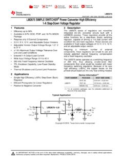
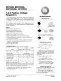
Transcription of Description Pin Assignments - Diodes Incorporated
1 AP1501 Document number: DS31014 Rev. 13 - 2 1 of 13 August 2020 Diodes Incorporated AP1501 150kHz, 3A PWM Buck DC/DC Converter Description The AP1501 is a fully integrated step-down DC/DC converter, with the ability to drive 3A load without the need of additional driver components. The AP1501 operates at a switching frequency of 150kHz enabling the use of small size filter components. As a result, board space is reduced and BOM costs are lowered. The AP1501 has integrated the shutdown function that allows standby mode to be activated via an external logic signal input. The internal compensation facilitates feedback control for line and load regulation without the need of an external circuitry. The AP1501 has a built-in Thermal shutdown and Current Limit function to prevent damage from high operating temperature and high current operating to the output switch.
2 Additional features include a guaranteed +/- 4% tolerance on the output voltage under specified input and output load conditions, and +/- 15% on oscillator frequency. The AP1501 offers both fixed and a Adjustable output voltages. For fixed outputs the AP1501 supports , and 12V. The package options available are standard 5-lead TO263 and TO220(R) packages. Features Output voltage : , 5V, 12V and Adjustable Output Version Adjustable Version Output voltage Range, to 37V+4% 150kHz +15% Fixed Switching Frequency voltage Mode Non-Synchronous PWM Control Thermal-Shutdown and Current-Limit Protection ON/OFF Shutdown Control Input Operating voltage can be up to 40V Output Load Current: 3A Low Power Standby Mode Built-In Switching Transistor on Chip TO263-5 and TO220-5(R) Packages Totally Lead-Free & Fully RoHS Compliant (Notes 1 & 2) Halogen- and Antimony-Free.
3 Green Device (Note 3) Pin Assignments ( Top View )1 VIN5 SD4 FB3 Gnd2 OutputMetal Tab GNDTO263-5L 1 VIN5 SD4 FB3 Gnd2 Output( Top View )TO220-5L/TO220-5L(R) Applications Simple High-Efficiency Step-Down Regulator On-Card Switching Regulators Positive to Negative Converter Notes: 1. No purposely added lead. Fully EU Directive 2002/95/EC (RoHS), 2011/65/EU (RoHS 2) & 2015/863/EU (RoHS 3) compliant. 2. See for more information about Diodes Incorporated s definitions of Halogen- and Antimony-free, "Green" and Lead-free. 3. Halogen- and Antimony-free "Green products are defined as those which contain <900ppm bromine, <900ppm chlorine (<1500ppm total Br + Cl) and <1000ppm antimony compounds. AP1501 Document number: DS31014 Rev. 13 - 2 2 of 13 August 2020 Diodes Incorporated AP1501 1235412 VDC Load Typical Applications Circuit (1) Fixed Type Circuit Typical Applications Circuit (continued) (2) Adjustable Type Circuit 1235412 VDC InputCinCapacitorFBSDD1(Note 5)VinGndOutputAP1501 CoCapacitorL1 47uH5V/ 3 AOutput LoadR2R1 Vout = VFB (1 +R2R1) VFB = R2 = 1K ~ 3K (3) Delay Start Circuit 1235412 VDC InputCinCapacitorFBSDD1(Note 5)VinGndOutputAP1501 CoCapacitorL1 47uH5V/ 3 AOutput LoadR2R1 Note: Suggested Diodes Incorporated s Power Schottky: B340A or PDS340 series.
4 AP1501 Document number: DS31014 Rev. 13 - 2 3 of 13 August 2020 Diodes Incorporated AP1501 Pin Descriptions Name Description VIN Operating voltage Input Output Switching Output Gnd Ground FB Output voltage Feedback Control SD ON/OFF Shutdown Functional Block Diagram ++_+_ThermalShutdownPre-driverCompCompGn dOutputVINSDFB220mV200mV3 ASwitch+__AmpCompFrequencycompen-sation AP1501 Document number: DS31014 Rev. 13 - 2 4 of 13 August 2020 Diodes Incorporated AP1501 Absolute Maximum Ratings Symbol Parameter Rating Unit ESD MM Machine Model ESD Protection 400 V VCC Supply voltage +45 V VSD ON/OFF Pin Input voltage to +40 V VFB Feedback Pin voltage to +40 V VOUT Output voltage to Ground -1 V PD Power Dissipation Internally Limited W TST Storage Temperature -65 to +150 C TJ Operating Junction Temperature -20 to +125 C TMJ Maximum Junction Temperature +150 C AP1501 Document number: DS31014 Rev.
5 13 - 2 5 of 13 August 2020 Diodes Incorporated AP1501 Electrical Characteristics (@ TA = +25 C, unless otherwise specified.) Unless otherwise specified, VIN = 12V for , 5V, adjustable version and VIN = 24V for the 12V version. ILOAD = Specifications with boldface type are for full operating temperature range, the other type are for TJ = +25 C. Symbol Parameter Conditions Min Typ. Max Unit IFB Feedback Bias Current VFB = (Adjustable Version Only) (Note 4) 40 60 nA 100 FOSC Oscillator Frequency 127 150 173 kHz 110 173 VSAT Saturation voltage IOUT = 3A No Outside Circuit VFB = 0V Force Driver On V DC Max. Duty Cycle (ON) VFB = 0V Force Driver On 100 % Min. Duty Cycle (OFF) VFB = 12V Force Driver Off 0 ICL Current Limit Peak Current No Outside Circuit VFB = 0V Force Driver On A IL Output = 0 Output Leakage Current 200 200 A Output = -1 2 60 60 mA IQ Quiescent Current VFB = 12V Force Driver Off 5 10 mA ISTBY Standby Quiescent Current ON/OFF Pin = 5V VIN = 40V 150 250 A 350 VIL ON/OFF Pin Logic Input Threshold voltage Low (Regulator ON) V VIH High (Regulator OFF) IH ON/OFF Pin Logic Input Current VLOGIC = (OFF) 15 25 A IL ON/OFF Pin Input Current VLOGIC = (ON) 5 JA Thermal Resistance Junction to Ambient TO263-5 (Note 5) 37 C/W TO220-5(R) (Note 5) 31 JC Thermal Resistance Junction to Case TO263-5 (Note 5) 6 C/W TO220-5(R) (Note 5) 5 Notes: 4.
6 Feedback pin removed from output and connected to 0V to force the output transistor switch ON. Feedback pin removed from output and connected to 12V for the , 5V, and the ADJ. version, and 15V for the 12V version, to force the output transistor switch OFF. 5. Test condition: Device mounted with copper area of approximately 3 in2,1oz, no air flow. AP1501 Document number: DS31014 Rev. 13 - 2 6 of 13 August 2020 Diodes Incorporated AP1501 Electrical Characteristics (continued) (@ TA = +25 C, unless otherwise specified.) Specifications with boldface type are for full operating temperature range, the other type are for TJ = +25 C. Symbol Parameter Conditions VMin Typ. VMax Unit AP1501-ADJ FBV Output Feedback < VIN < 40V < ILOAD < 3A VOUT programmed for 3V V Efficiency VIN = 12V, ILOAD = 3A 73 % OUTV Output voltage < VIN < 40V < ILOAD < 3A V Efficiency VIN = 12V, ILOAD = 3A 73 % AP1501-5V OUTV Output voltage 7V < VIN < 40V < ILOAD < 3A 5 V Efficiency VIN = 12V, ILOAD = 3A 80 % AP1501-12V OUTV Output voltage 15V < VIN < 40V < ILOAD < 3A 12 V Efficiency VIN = 15V, ILOAD = 3A 90 % AP1501 Document number: DS31014 Rev.
7 13 - 2 7 of 13 August 2020 Diodes Incorporated AP1501 Performance Characteristics Typical Performance CharacteristicsNormalized Output voltage (V)VIN=20V, ILOAD=3 ANormalized at TJ=25oCJUNCTION TEMPERATURE(oC)JUNCTION TEMPERATURE(oC)SWITCH CURRENT LIMIT (A)Switch Current TEMPERATURE(oC)SUPPLY CURRENT (mA)Operating Quiescent CurrentJUNCTION TEMPERATURE(oC)EFFICIENCY (%) CURRENT(A)SATURATION voltage (V)1231 : -40oC2 : 25oC3 : 125oCSwitch Saturation , VOUT=5 VSUPPLY VOLOTAGE (V)CURRENT (uA) Quiescent Current10203040 VON/OFF=5V1 : -40oC2 : 25oC3 : 125oC132 Switch ONSwitch OFF AP1501 Document number: DS31014 Rev. 13 - 2 8 of 13 August 2020 Diodes Incorporated AP1501 Performance Characteristics (continued) JUNCTION TEMPERATURE(oC)BIAS CURRENT (nA)Feedback Pin Bias PIN voltage (V)CURRENT (uA)ON/OFF Pin Current (Sinking) TJ 125oC Version TEMPERATURE (oC)SUPPLY voltage (V)Minimum Operating Supply VoltageVOUT= TEMPERATURE (oC)THRESHOLD voltage (V)ON/OFF Threshold FrequencyJUNCTION TEMPERATURE (oC)FREQUENCY (kHz) AP1501 Document number: DS31014 Rev.
8 13 - 2 9 of 13 August 2020 Diodes Incorporated AP1501 Ordering Information AP1501 - XX XXX X - X Output version Package Lead Free Packing Blank : Adjustable K5 : TO263-5 L : Lead Free U : Tube 33 : T5 : TO220-5 G : Green 13 : Tape & Reel 50 : T5R : TO220-5(R) 12 : 12V Device (Note 4) voltage Package Code Package (Note 7) Lead Free/ Green Quantity Part Number Suffix Status (Note 6) Tube 13 Tape and reel AP1501-50K5G-13 50 K5 TO263-5 Green 800 NA -13 Active AP1501-K5G-13 ADJ K5 TO263-5 Green 800 NA -13 Active AP1501-12K5G-13 12 K5 TO263-5 Green 800 NA -13 NRND AP1501-33K5G-13 33 K5 TO263-5 Green 800 NA -13 NRND Notes: 6. AP1501-50K5G-13 and AP1501-K5G-13 are Active. All other versions are NRND or EOL. For recommended alternatives to NRND/EOL devices, Contact Us.
9 7. For packaging details, go to our website at: Operation Description Pin Functions +VIN This is the positive input supply for the IC switching regulator. A suitable input bypass capacitor must be present at this pin to minimize voltage transients and to supply the switching currents needed by the regulator. Ground Circuit ground. Output Internal switch. The voltage at this pin switches between (+VIN VSAT) and approximately , with a duty cycle of approximately VOUT / VIN. To minimize coupling to sensitive circuitry, the PC board copper area connected to this pin should be kept a minimum. Feedback Senses the regulated output voltage to complete the feedback loop. ON/OFF Allows the switching regulator circuit to be shutdown using logic level signals thus dropping the total input supply current to approximately 150 A. Pulling this pin below a threshold voltage of approximately turns the regulator on, and pulling this pin above (up to a maximum of 40V) shuts the regulator down.
10 If this shutdown feature is not needed, the ON/OFF pin can be wired to the ground pin or it can be left open, in either case the regulator will be in the ON condition. Thermal Considerations The AP1501 is available in 5-pin surface mount TO-263 and TO-220. The TO-220 package needs a heat sink under most conditions. The size of the heat sink depends on the input voltage , the output voltage , the load current and the ambient temperature. The AP1501 junction temperature rises above ambient temperature for a 3A load and different input and output voltages. The data for these curves was taken with the AP1501 (TO-220 package) operating as a buck switching regulator in an ambient temperature of 25 C (still air). These temperature rise numbers are all approximate and there are many factors that can affect these temperatures. Higher ambient temperatures require more heat sinking.