Transcription of Design With PIN Diodes Application Note, …
1 Application NOTE. Design with PIN Diodes Introduction The PIN diode finds wide usage in RF, UHF, and microwave circuits. At these types of frequencies, a PIN diode is fundamentally a device with an impedance controlled by its DC. excitation. A unique feature of the PIN diode is its ability to control large amounts of RF power with much lower levels of DC. This Application Note describes the use of PIN Diodes in circuit Design . PIN diode Fundamentals The PIN diode is a current-controlled resistor at radio and microwave frequencies. It is a silicon semiconductor diode in Figure 1. PIN diode Cross-Section which a high-resistivity, intrinsic I region is sandwiched between a P-type and N-type region. When the PIN diode is forward biased, There is a common misconception that carrier lifetime, , is the holes and electrons are injected into the I region.
2 These charges only parameter that determines the lowest frequency of operation do not immediately annihilate each other; instead they stay alive and the distortion produced. This is indeed a factor, but equally for an average time, called the carrier lifetime, t. This results in an important is the thickness of the I region, W, which relates to the average stored charge, Q, which lowers the effective resistance of transit time frequency of the PIN diode . the I region to a value RS. When the PIN diode is at zero or reverse bias, there is no stored charge in the I region and the diode appears as a capacitor, CT, Low-Frequency Model shunted by a parallel resistance RP. At low frequencies (below the transit time frequency of the PIN Diodes are described using the following parameters: I region) and DC, the PIN diode behaves like a silicon PN junction RS series resistance under forward bias semiconductor diode .
3 Its I-V characteristic (see Figure 2). determines the DC voltage at the forward bias current level. PIN. CT total capacitance at zero or reverse bias Diodes are often rated for the forward voltage, VF, at a fixed DC. RD parallel resistance at zero or reverse bias bias. VR maximum allowable DC reverse bias voltage The reverse voltage, VR, rating of a PIN diode is a guarantee from carrier lifetime the manufacturer that no more than a specified amount, generally 10 A, of reverse current is present when VR is applied. It is not AV average thermal resistance or: necessarily the avalanche or bulk breakdown voltage, VB, PD maximum average power dissipation determined by the I region width (approximately 10 V/mm). PIN. PULSE pulse thermal impedance or: Diodes of the same bulk breakdown voltage may have different voltage ratings.
4 Generally, the lower the voltage rating, the less PP maximum peak power dissipation expensive the PIN diode . By varying the I region width and diode area, it is possible to construct PIN Diodes of different geometries that result in the same RS and CT characteristics. These devices may have similar small signal characteristics. However, the thicker I region diode would have a higher bulk, or RF breakdown voltage, and better distortion properties. On the other hand, the thinner device would have faster switching speed. Skyworks Solutions, Inc. Phone [781] 376-3000 Fax [781] 376-3100 200312D Skyworks Proprietary Information Products and Product Information are Subject to Change Without Notice October 22, 2012 1. Application NOTE Design with PIN Diodes . In commercially available Diodes , the parasitic resistance of the diode package and contacts limit the lowest resistance value.
5 The lowest impedance is affected by the parasitic inductance, L, which is generally less than 1 nH. Equation (2) is valid at frequencies higher than the I region transmit time frequency, according to the following relationship: 1300. f > (where f is in MHz and W in m) (3). W2. For this equation, it is assumed that the RF signal does not affect the stored charge. Zero or Reverse Bias Model A. CT = (4). W. Where: = dielectric constant of silicon A = area of diode junction Figure 2. Typical PIN diode I-V Characteristics Equation (4) is valid at frequencies above the dielectric relaxation frequency of the I region, according to the following relationship: Large Signal Model 1. f > (where is the resistivity of the I region) (5). When the PIN diode is forward biased, the stored charge, Q, must 2.
6 Be much greater than the incremental stored charge added or At lower frequencies, the PIN diode acts like a varactor. In these removed by the RF current, IRF. To ensure this, the following cases, the value RP is proportional to voltage and inversely inequality must hold: proportional to frequency. In most RF applications , its value is I RF higher than the reactance of the capacitance, CT, and is less Q >> (1). 2 f significant. Under reverse bias, the diode should not be biased beyond its DC. voltage rating, VR. The avalanche or bulk breakdown voltage, VB, RF Electrical Modeling of the PIN diode of a PIN diode is proportional to the I region width, W, and is always higher than VR. Forward Bias Model In a typical Application , the maximum negative voltage swing W2. RS = ( ) should never exceed VB.
7 An instantaneous excursion of the RF. (. n + p Q ) (2). signal into the positive bias direction generally does not cause the diode to go into conduction because of slow reverse to forward Where: Q = IF (in coulombs) switching speed. W = I region width IF = forward bias current The DC reverse bias needed to maintain low PIN diode = carrier lifetime conductance has been analyzed(1) and is related to the magnitude n = electron mobility of the RF signal and I region width. p = hole mobility Skyworks Solutions, Inc. Phone [781] 376-3000 Fax [781] 376-3100 2 October 22, 2012 Skyworks Proprietary Information Products and Product Information are Subject to Change Without Notice 200312D. Application NOTE Design with PIN Diodes . Switching Speed Model Thermal Model The switching speed in any Application depends on the driver The maximum allowable power dissipation, PD, is determined by circuit as well as the PIN diode .
8 Certain primary PIN properties can the following equation: influence switching speed. TJ TA. A PIN diode has two switching speeds from forward bias to PD = (7).. reverse bias, TFR, and from reverse bias to forward bias, TRF. The diode characteristic that affects TFR is , carrier lifetime. The value Where: PD = power dissipation in Watts. of TFR may be computed from the forward current, IF, and the TJ = maximum allowable junction temperature (usually initial reverse current, IR, as follows (and illustrated in Figure 3): 175 C). I TA = ambient or heat sink temperature. TFR = log e 1 + F (6). IR Power dissipation may be computed as the product of the RF. current squared, multiplied by the diode resistance, RS. Where TFR is measured in seconds. For Continuous Wave (CW) applications , the value of thermal resistance, , used is the average thermal resistance, AV.
9 In most pulsed RF and microwave applications where the Duty Factor (DF) is less than 10 percent and the pulse width, TP, is less than the thermal time constant of the diode , good approximation of the effective value of in Equation (7) may be computed as follows: = DF AV + TP (8). Where: = thermal resistance in C/W. TP = thermal impedance of the diode for the time interval corresponding to TP. Figure 4 indicates how junction temperature is affected during a pulsed RF Application . Figure 3. diode Current vs Time The reverse bias to forward bias time, TRF, depends primarily on I. region width, W, as indicated in the following Table of typical data: To 10 mA To 50 mA To 100 mA. I-Width From: From: From: ( m) 10 V 100 V 10 V 100 V 10 V 100 V. ( s) ( s) ( s) ( s) ( s) ( s). 175 100 50 Figure 4.
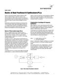
10 Power Dissipation and Junction Temperature vs Time Skyworks Solutions, Inc. Phone [781] 376-3000 Fax [781] 376-3100 200312D Skyworks Proprietary Information Products and Product Information are Subject to Change Without Notice October 22, 2012 3. Application NOTE Design with PIN Diodes . PIN diode applications Switches PIN Diodes are commonly used as switching elements to control RF signals. In these applications , the PIN diode can be biased to either a high or low impedance device state, depending on the level of stored charge in the I region. A simple untuned Single Pole, Single Throw (SPST) switch may be designed using either a single series or shunt connected PIN. diode , as shown in Figure 5. The series connected diode switch is commonly used when minimum insertion loss is required over a broad frequency range.