Transcription of Diffraction Based Overlay Metrology for Double Patterning ...
1 22. Diffraction Based Overlay Metrology for Double Patterning technologies Prasad Dasari1, Jie Li1, Jiangtao Hu1, Nigel Smith1 and Oleg Kritsun2. 1 Nanometrics 2 Globalfoundries USA. 1. Introduction 193nm optical immersion lithography is approaching its minimum practical single-exposure limit of 80nm pitch [1]. The semiconductor industry has adopted Double Patterning technology (DPT) as an attractive solution for the low k1 regime until extreme ultraviolet (EUV) lithography becomes commercialized. DPT also brings additional demands of increased critical dimension uniformity (CDU) and decreased Overlay errors. The International Technology Roadmap for Semiconductors (ITRS) [2] target for Overlay control at the 32nm DRAM node in single patterned lithography steps is 6nm.
2 The process budget is reduced to for DPT. If 20% of the process error budget is allowed to occur in the Metrology tool, as the ITRS states, then the measurement error budget at the 32nm node is for single Patterning , and for DPT. The ITRS defines total measurement uncertainty (TMU) for Overlay only in terms of precision, tool-induced shift (TIS) variation and site-to-site tool matching differences. Determining whether a measurement technology is capable of controlling these advanced processes is no longer a case of simple data self-consistency checks on precision, TIS and matching. For example, the error arising from assumptions of a linear change of Overlay error with position is significant.
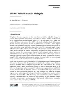
3 This error can be reduced by using very small targets [3] and performing in-device Overlay measurements, but the demanding sub-nanometer measurement budget in Overlay measurements still remains a considerable challenge. Recent advances in lithography Metrology for advanced Patterning have led to the proposal of three different pitch splitting technologies [Fig. 1]. The Litho-Etch-Litho-Etch method (LELE, Fig. 1a) involving two process steps requires very tight Overlay control and is both very expensive and slow, making alternative methods attractive. The first alternative process flow is Litho-Freeze-Litho-Etch (LFLE), which reduces the processing cost by replacing the intermediate etch step with a process step in the litho track (Fig.)
4 1b). After exposing the first pattern, the resist is baked in a post-exposure bake (PEB) step and developed. Exposed pattern is coated with material to freeze the resist. The second resist layer is added and the second exposure is done. The freezing material prevents the first resist layer from washing away during the second layer PEB and develop steps. This 434 Recent Advances in Nanofabrication Techniques and Applications technique allowed printing 2D logic cells and dense poly lines with two lithography steps, illustrating good resolution and process margin [4]. The next alternative process is Self-Aligned Double Patterning (SADP, Fig. 1c), in which a spacer film is formed on the sidewalls of pre-patterned features.
5 Etching removes all the material of the original pattern, leaving only the spacer material. Since there are two spacers for every line, the line density has now doubled. The spacer approach is unique in that with one lithographic exposure the pitch can be halved indefinitely with a succession of spacer formation and pattern transfer processes. The spacer film deposition process is very uniform and results in extremely good SADP CDU of less than 1nm. The spacer lithography technique has most frequently been applied in Patterning fins for FinFETs and metal layers [5]. (a) (b) (c). Fig. 1. Various Double Patterning schemes: (a) Litho-etch-litho-etch (LELE), (b) Litho-freeze- litho-etch (LFLE), and (c) Self-aligned Double Patterning (SADP).
6 These pitch splitting Double Patterning techniques not only involve more demanding process steps, they also require tighter Overlay control than conventional single Patterning [2]. Therefore measurement of Overlay with much higher certainty is a necessity. As technology transitions toward the 22nm and 16nm nodes using these methods there is serious concern about the capability of the available Metrology solutions, both in process development and production control. High TIS and tool-to-tool matching errors make it difficult to meet the measurement uncertainty requirements using the traditional Image- Based Overlay method (IBO), even though most advanced IBO tools are operating at TMU levels under 1nm.
7 Diffraction - Based (scatterometry) Overlay (DBO) measurement is an alternative optical measurement technique that has been reported to offer better precision than IBO and near zero TIS [6, 12, 14-15], and is therefore a possible solution to the measurement uncertainty budget. Bischoff et al. proposed measuring Overlay using the Diffraction efficiencies of the first diffracted orders [7]. Chun-Hung Ko used angular scatterometry combined with an experimental library to determine the Overlay error on ADI stacks with intermediate poly-silicon lines [8]. Huang et al. used spectra from reflection symmetry gratings and a rigorous coupled- Diffraction Based Overlay Metrology for Double Patterning technologies 435.
8 Wave analysis (RCWA) regression approach to calculate the Overlay error [9]. W. Yang et al. [10] and D. Kandel et al. [11] used arrays of specially constructed pads with programmed offsets to determine Overlay without the need for model fitting. These DBO methods have the potential to meet the demanding Overlay Metrology budget for sub-32nm technology nodes. In this chapter, the advantages of DBO for precise and accurate Overlay measurement in LELE, LFLE and SADP processes will be shown. 2. Spectroscopic scatterometry Experimental setup Spectroscopic scatterometry is used to measure Overlay errors between stacked periodic structures ( , gratings). In this technique, broadband linearly polarized light is incident perpendicular to the wafer surface and the zero-order diffracted signal (spectrum) is measured as a function of wavelength.
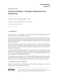
9 Fig. 2 shows a typical experimental configuration. At normal incidence, different reflectance spectra are obtained for various angles of polarization with respect to that of the periodic structure. Typical data collection involved both TE and TM spectra. A specific advantage of using polarized light is that it provides enhanced sensitivity as both the amplitude and phase differences between the TE and TM. spectra can be measured. (b). (a) (c). Fig. 2. The figure shows a typical hardware set up for a normal incidence scatterometer (a). spectroscopic reflectometry, (b) normal incidence reflection, and (c) TE TM data acquisition modes. Theory Spectra are obtained from pads, each of which has gratings patterned in both layers between which the Overlay error is being measured (Fig.)
10 3). The gratings in each pad are overlaid but by design shifted with respect to each other. Spectra from pads with shifts of equal magnitude but opposite direction are identical due to symmetry: 436 Recent Advances in Nanofabrication Techniques and Applications R( x0 , ) R( x0 , ) (1). Here R(x0 ) is the reflectance spectrum from one pad as a function of wavelength and shift +x0. The difference spectra ( R( )=R(+x0, ) - R(-x0, )) from two pads with shifts +x0. and -x0 is zero in the absence of noise in the measuring tool. A small Overlay error shifts both upper gratings in the same direction and breaks the symmetry. The resulting differential spectrum is proportional to the direction and magnitude of the Overlay error: R.