Transcription of DN2535 N-Channel Depletion-Mode Vertical …
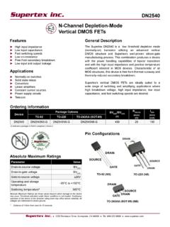
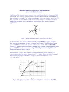
1 1235 Bordeaux Drive, Sunnyvale, CA 94089 Tel: 408-222-8888 = Lot NumberYY = Year SealedWW = Week Sealed = Green PackagingDN2535N5 LLLLLLLLLYYWWF eaturesHigh input impedanceLow input capacitanceFast switching speedsLow on-resistanceFree from secondary breakdownLow input and output leakageApplicationsNormally-on switchesSolid state relaysConvertersLinear amplifiersConstant current sourcesPower supply circuitsTelecom General DescriptionThe Supertex DN2535 is a low threshold depletion mode (normally-on) transistor utilizing an advanced Vertical DMOS structure and Supertex s well-proven silicon-gate manufacturing process. This combination produces a device with the power handling capabilities of bipolar transistors and with the high input impedance and positive temperature coefficient inherent in MOS devices.
2 Characteristic of all MOS structures, this device is free from thermal runaway and thermally-induced secondary s Vertical DMOS FETs are ideally suited to a wide range of switching and amplifying applications where high breakdown voltage, high input impedance, low input capacitance, and fast switching speeds are depletion -ModeVertical DMOS FETsOrdering InformationDevicePackage OptionsBVDSX/BVDGX(V)RDS(ON)(max)( )IDSS(min)(mA)TO-92TO-220DN2535DN2535N3- GDN2535N5-G35025150-G indicates package is RoHS compliant ( Green )Absolute Maximum Ratings ParameterValueDrain-to-source voltageBVDSXD rain-to-gate voltageBVDGXGate-to-source voltage 20 VOperating and storage temperature-55OC to +150 OCSoldering temperature* 300 OCAbsolute Maximum Ratings are those values beyond which damage to the device may occur. Functional operation under these conditions is not implied.
3 Continuous operation of the device at the absolute rating level may affect device reliability. All voltages are referenced to device ground.* Distance of from case for 10 Configurations Product Marking 3-Lead TO-220 (N5)3-Lead TO-92 (N3)YY = Year SealedWW = Week Sealed = Green Packaging DN2 5 3 5 YYWW3-Lead TO-220 (N5)3-Lead TO-92 (N3)GATESOURCEDRAINGATESOURCEDRAINDRAIN2 DN2535 1235 Bordeaux Drive, Sunnyvale, CA 94089 Tel: 408-222-8888 CharacteristicsPackageID (continuous) (mA)ID (pulsed)(mA)Power Dissipation@TC = 25OC(W) jc(OC/W) ja(OC/W)IDR (mA)IDRM(mA) : ID (continuous) is limited by max rated Characteristics (TA = 25OC unless otherwise specified)SymParameterMinTypMaxUnitsCond itionsBVDSXD rain-to-source breakdown voltage350--VVGS = , ID = 100 AVGS(OFF)Gate-to-source off = 25V, ID = 10 A VGS(OFF)Change in VGS(OFF) with = 25V, ID = 10 AIGSSGate body leakage current--100nAVGS = 20V, VDS = 0 VID(OFF)Drain-to-source leakage current--10 AVDS = Max rating, VGS = = Max Rating, VGS = -10V, TA = 125 OCIDSSS aturated drain-to-source current150--mAVGS = 0V, VDS = 25 VRDS(ON)Static drain-to-source on-state resistance-1725 VGS = 0V, ID = 120mA RDS(ON)Change in RDS(ON) with = 0V, ID = 120mAGFSF orward transconductance-325-mmho VDS = 10V, ID = 100mACISSI nput capacitance-200300pFVGS = -10V,VDS = 25V,f = source output capacitance-1230 CRSSR everse transfer (ON)
4 Turn-on delay time--10nsVDD = 25V,ID = 150mA,RGEN = 25 ,trRise time--15td(OFF)Turn-off delay time--15tfFall time--20 VSDD iode forward voltage = -10V, ISD = 120mAtrrReverse recovery time-800-nsVGS = -10V, ISD = :All parameters 100% tested at 25OC unless otherwise stated. (Pulse test: 300 s pulse, 2% duty cycle.)All parameters sample Waveforms and Test Circuit90%10%90%90%10%10% (ON)td(ON)t(OFF)td(OFF)tFtrINPUTINPUTOUT PUT0 VVDDRGEN0V-10V3DN2535 1235 Bordeaux Drive, Sunnyvale, CA 94089 Tel: 408-222-8888 Performance CurvesOutput (volts)Transconductance vs. Drain CurrentPower Dissipation vs. Ambient Temperature015010050102001257525TO-220TO -92 VGS = Characteristics250200150100500012354 VGS = Rated Safe Operating (pulsed)TC = 25 C(TA = 25 C)TO-220 (DC)TO-92 (DC)Thermal Response Characteristics)dezilamron( ecnatsiseR 150200 VDS= 10 VTA = -55 CTA = 25 CTA = 125 CTO-220TC = 25 CPD = 15 WTO-92TC = 25 CPD = (A52 = )CID)serepma( ID)spmaillim( VDS (volts)GSF)snemeis( ID (milliamps)TC ( C)PD)sttaw( VDS (volts)ID)serepma( tp (seconds)4DN2535 1235 Bordeaux Drive, Sunnyvale, CA 94089 Tel: 408-222-8888 Performance Curves (cont.)
5 BVDSS Variation with TemperatureVBSSD dezilamroN CharacteristicsVGS (Volts)VDS (Volts)ID)serepma( Vs. Drain-to-Source Voltage)sdarafociP( C200150100500010203040 VGS = -5 VVGS= 0 VVDS = 10 VVGS = -10 VCOSSCRSSCISSTA = -55 CTA = 25 CRDS (ON)@ ID = 120mAVGS(OFF)@ 10 AVDS= 20 VVDS= 40V200pF170pFTA = 125 COn-Resistance vs. Drain Current100806040200QC (Nanocoulombs)R)no(SD)smhO( (off) and RDS Variation with ( C)dezilamroNGate Drive Dynamic CharacteristicsVSG)stloV( Tj ( C)ID (milliamps)5DN2535 1235 Bordeaux Drive, Sunnyvale, CA 94089 Tel: 408-222-8888 TO-92 Package Outline (L/LL/N3)SymbolAbcDEE1ee1 LDimensions(inches) .014 ..022 . *JEDEC Registration TO-92.* This dimension is not specified in the original JEDEC drawing. The value listed is for reference only. This dimension is a non-JEDEC not to Doc.#: DSPD-3TO92N3, Version Plane123 Front ViewSide ViewBottom ViewE1 EDe1 Lec1 2 3bASupertex inc.
6 Does not recommend the use of its products in life support applications, and will not knowingly sell them for use in such applications unless it receives an adequate product liability indemnification insurance agreement. Supertex inc. does not assume responsibility for use of devices described, and limits its liability to the replacement of the devices determined defective due to workmanship. No responsibility is assumed for possible omissions and inaccuracies. Circuitry and specifications are subject to change without notice. For the latest product specifications refer to the Supertex inc. website: 2008 All rights reserved. Unauthorized use or reproduction is Bordeaux Drive, Sunnyvale, CA 94089 Tel: 408-222-8888www . (The package drawing(s) in this data sheet may not reflect the most current specifications. For the latest package outline information go to )Doc.
7 # DSFP- DN2535 B1031083-Lead TO-220 Package Outline (N5)SymbolAA1A2bb2cDD1D2EE1E2eH1LL1Q PDimen-sion(inches) ..474 . *. *.. Registration TO-220, Variation AB, Issue K, April 2002.* This dimension is not specified in the original JEDEC drawing. The value listed is for reference only. This dimension is a non-JEDEC not to Doc. #: DSPD-3TO220N5, Version PSeatingPlaneA1 AAChamferOptionalH1ED2 ThermalPadFront ViewSide ViewView A - AL1bb2123E1 View Bc