Transcription of Dual-Channel Synchronous DC/DC Step-Down Controller …
1 RT8249A/B/C DS8249A/B/C-02 June 2014 Richtek Technology Corporation. All rights reserved. is a registered trademark of Richtek Technology Corporation. Simplified Application CircuitGeneral DescriptionThe RT8249A/B/C is a Dual-Channel Step-Down , controllergenerating supply voltages for battery-powered includes two Pulse-Width Modulation (PWM) controllersadjustable from 2V to , and two fixed 5 linearregulators. Each linear regulator provides up to 100mAoutput current and linear regulator provides 1%accuracy under 35mA. The RT8249A/B has an oscillatoroutput to driver the external charge pump application. TheRT8249C provides a mode selection pin, SKIPSEL, toselect Diode-Emulation Mode (DEM) or Audio SkippingMode (ASM).
2 Other features include on-board power-upsequencing, a power-good output, internal soft-start, andsoft-discharge output that prevents negative voltage constant current ripple PWM control scheme operateswithout sense resistors and provides 100ns response toload transient. For maximizing power efficiency, theRT8249A/B/C automatically switches to the diode-emulation mode in light load applications. The RT8249A/B/C is available in the WQFN-20L 3x3 Support Connected Standby Mode for Ultrabook CCRCOT Control with 100ns Load Step Response PWM Maximum Duty Ratio > 98% 5V to 25V Input Voltage Range 2V to Output Voltage Range 5 LDOs with 100mA Output current 1% Accuracy on LDO Output Oscillator Driving Output for Charge PumpApplication Internal Frequency Setting RT8249A/B : 400kHz/475kHz (CH1/CH2) RT8249C.
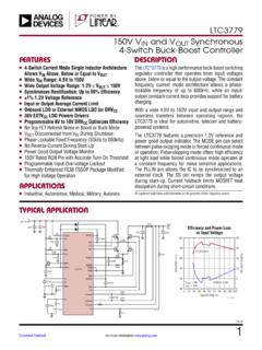
3 500kHz/600kHz (CH1/CH2) Internal Soft-Start and Soft-Discharge 4700ppm/ C RDS(ON) current Sensing Independent Switcher Enable Control Built in OVP/UVP/OCP/OTP Non-latch UVLO Power Good Indicator 20-Lead WQFN Package RoHS Compliant and Halogen FreeDual-Channel Synchronous DC/DC Step-Down Controllerwith 5 LDOsRT8249A/ 1 EnableEN2 Channel 2 EnableLDO55 VPGOOD IndicatorCS1CS2 GNDOffOnRT8249A/B/C2DS8249A/B/C-02 June Copyright 2014 Richtek Technology Corporation. All rights reserved. is a registered trademark of Richtek Technology InformationNote :**Empty means Pin1 orientation is Quadrant 1 Richtek products are : RoHS compliant and compatible with the current require- ments of IPC/JEDEC J-STD-020.
4 Suitable for use in SnPb or Pb-free soldering ConfigurationsRT8249A/B(TOP VIEW)Marking Information2Q= : Product CodeYMDNN : Date Code2P= : Product CodeYMDNN : Date Code2N= : Product CodeYMDNN : Date CodeRT8249 CWQFN-20L 3x3RT8249 AGQWRT8249 BGQWRT8249 CGQWA pplications Notebook and Sub-Notebook Computers System Power Supplies 3-Cell and 4-Cell Li+ Battery-Powered Devices2Q=YMDNN2P=YMDNN2N=YMDNNFB2 LDO3CS1FB1 LGATE1 BYP1 VINLDO5EN2 PGOODBOOT2EN1 VCLKBOOT1 PHASE1 UGATE1CS2 LGATE2 UGATE2 PHASE2151413121718192012349876 GND211151610FB2 LDO3CS1FB1 LGATE1 BYP1 VINLDO5EN2 PGOODBOOT2EN1 SKIPSELBOOT1 PHASE1 UGATE1CS2 LGATE2 UGATE2 PHASE2151413121718192012349876 GND211151610RT8249A/B/CPackage TypeQW : WQFN-20L 3x3 (W-Type)Lead Plating SystemG : Green (Halogen Free and Pb Free)Pin Function WithA : VCLK, LDO3 Always OnB : VCLK, LDO3/LDO5 Always OnC : SKIPSEL, LDO3 Always OnPin 1 Orientation**(2) : Quadrant 2, Follow EIA-481-DRT8249A/B/C3DS8249A/B/C-02 June Copyright 2014 Richtek Technology Corporation.
5 All rights reserved. is a registered trademark of Richtek Technology Pin DescriptionP in No. Pin Name Pin Function 1 CS 1 current Limit Setting. Connect a resistor to GND to set the threshold for Channel 1 Synchronous RDS(ON) sense. The GND PHASE1 current limit threshold is 1/8th the voltage seen at CS1 over a to 2V range. There is an internal 50 A current source from LDO5 to CS1. 2 F B1 Feedback Voltage Input for Channel 1. Connect FB1 to a resistive voltage divider from VOUT1 to GND to adjust output from 2V to 3 LDO3 Linear Regulator Output. It is always on when VIN is higher than VINPOR threshold.
6 4 F B2 Feedback Voltage Input for Channel 2. Connect FB2 to a resistive voltage divider from VOUT2 to GND to adjust output from 2V to 5 CS 2 current Limit Setting. Connect a resistor to GND to set the threshold for Channel 2 Synchronous RDS(ON) sense. The GND PHASE2 current limit threshold is 1/8th the voltage seen at CS2 over a to 2V range. There is an internal 50 A current source from LDO5 to CS2. 6 EN2 Enable Control Input for Channel 2. 7 PGOOD Power Good Indicator Output for Channel 1 and Channel 2. (Logical AND) 8 PH ASE 2 Switch Node of Channel 2 MOSFETs. PHASE2 is the internal lower supply rail for the UGATE2 high-side gate driver.
7 PHASE2 is also the current -sense input for the Channel 2. 9 BOOT2 Bootstrap Supply for Channel 2 High-Side Gate Driver. Connect to an external capacitor according to the typical application circuits. 10 UGATE2 High-Side Gate Driver Output for Channel 2. UGATE2 swings between PHASE2 and BOOT2. 11 LGATE2 Low-Side Gate Driver Output for Channel 2. LGATE2 swings between GND and LD O5. 12 VIN Power Input for 5V and LDO Regulators and Buck Controllers. 13 LDO5 5V Linear Regulator Output. LDO5 is also the supply voltage for the low-side MOSFET and analog supply voltage for the device. 14 BYP1 Switch-over Source Voltage Input for LDO5.
8 15 LGATE1 Low-Side Gate Driver Output for Channel 1. LGATE1 swings between GND and LD O5. 16 UGATE1 High-Side Gate Driver Output for Channel 1. UGATE1 swings between PHASE1 and BOOT1. 17 BOOT1 Bootstrap Supply for Channel 1 High-Side Gate Driver. Connect to an external capacitor according to the typical application circuits. 18 PHASE1 Switch Node of Channel 1 MOSFETs. PHASE1 is the internal lower supply rail for the UGATE1 high-side gate driver. PHASE1 is also the current sense input for the Channel 1. VC LK (RT8249A/B) Oscillator Output for Charge Pump. 19 SKIPSEL (RT8249C) PWM Operating Mode Selection.
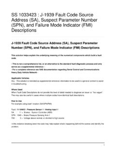
9 Diode-emulation Mode : Connect to LDO3 Audio Skipping Mode : Short to GND 20 EN1 Enable Control Input for Channel 1. 21 (Exposed Pad) GND Ground. The exposed pad must be soldered to a large PCB and connected to GND for maximum power dissipation. RT8249A/B/C4DS8249A/B/C-02 June Copyright 2014 Richtek Technology Corporation. All rights reserved. is a registered trademark of Richtek Technology Block DiagramOperationThe RT8249A/B/C includes two constant on-timesynchronous Step-Down controllers and two ControllerIn normal operation, the high-side N-MOSFET is turnedon when the output is lower than VREF, and is turned offafter the internal one-shot timer expires.
10 While the high-side N-MOSFET is turned off, the low-side N-MOSFET isturned on to conduct the inductor current until next internal soft-start function, an internal current sourcecharges an internal capacitor to build the soft-start rampvoltage. The output voltage will track the internal rampvoltage during soft-start power good output is an open-drain architecture. Whenthe two channels soft-start are both finished, the PGOOD open-drain output will be high LimitThe current limit circuit employs a unique valley currentsensing algorithm. If the magnitude of the current sensesignal at PHASE is above the current limit threshold, thePWM is not allowed to initiate a new cycle. Thus, thecurrent to the load exceeds the average output inductorcurrent, the output voltage falls and eventually crossesthe under-voltage protection threshold, inducing 2 Buck ControllerBOOT2 UGATE2 PHASE2 LGATE2 GNDLDO5FB2CS2 PGOODC hannel 1 Buck ControllerBOOT1 UGATE1 PHASE1 LGATE1 LDO5FB1CS1 LDO5 REFSW5 ThresholdVINLDO5 OSCVCLK (RT8249A/B)LDO3 LDO3 BYP1 Power-OnSequenceClear Fault LatchBYP1 BYP1 SKIPSEL (RT8249C)EN1EN2RT8249A/B/C5DS8249A/B/C-0 2 June Copyright 2014 Richtek Technology Corporation.