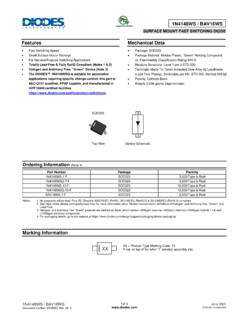
Transcription of Features Mechanical Data - Diodes Incorporated
1 BZT52C2V0 - BZT52C51 Document number: DS18004 Rev. 38 - 2 1 of 5 October 2017 Diodes Incorporated BZT52C2V0 - BZT52C51 SURFACE MOUNT ZENER DIODE Features Planar Die Construction 500mW Power Dissipation General Purpose, Medium Current Ideally Suited for Automated Assembly Processes Totally Lead-Free & Fully RoHS Compliant (Notes 1 & 2) Halogen and Antimony Free. Green Device (Notes 3 & 4) Qualified to AEC-Q101 Standards for High Reliability Mechanical Data Case: SOD123 Case Material: Molded Plastic. UL Flammability Classification Rating 94V-0 Moisture Sensitivity: Level 1 per J-STD-020 Terminals: Matte Tin Finish Annealed over Alloy 42 Leadframe (Lead Free Plating).
2 Solderable per MIL-STD-202, Method 208 Polarity: Cathode Band Weight: grams (Approximate) Ordering Information (Notes 5 & 6) Part Number Qualification Case Packaging (Type Number)-7-F Commercial SOD123 3,000/Tape & Reel (Type Number)Q-7-F Automotive SOD123 3,000/Tape & Reel (Type Number)-13-F Commercial SOD123 10,000/Tape & Reel (Type Number)Q-13-F Automotive SOD123 10,000/Tape & Reel Notes: 1. No purposely added lead. Fully EU Directive 2002/95/EC (RoHS) & 2011/65/EU (RoHS 2) compliant. 2. See for more information about Diodes Incorporated s definitions of Halogen- and Antimony-free, "Green" and Lead-free.
3 3. Halogen- and Antimony-free "Green products are defined as those which contain <900ppm bromine, <900ppm chlorine (<1500ppm total Br + Cl) and <1000ppm antimony compounds. 4. Product manufactured with Date Code V9 (week 33, 2008) and newer are built with Green Molding Compound. Product manufactured prior to Date Code V9 are built with Non-Green Molding Compound and may contain Halogens or Sb2O3 Fire Retardants. 5. For packaging details, go to our website at 6. For (Type Number), please see the Electrical Characteristics Table. Example: Zener = BZT52C6V2Q-13-F.
4 Marking Information Date Code Key Year 2013 2014 2015 2016 2017 .. 2020 2021 2022 2023 2024 Code A B C D E .. H I J K L Month Jan Feb Mar Apr May Jun Jul Aug Sep Oct Nov Dec Code 1 2 3 4 5 6 7 8 9 O N D Top View xx = Product Type Marking Code (See Electrical Characteristics Table) YM = Date Code Marking Y = Year (ex: E = 2017) M = Month (ex: 9 = September) SOD123 BZT52C2V0 - BZT52C51 Document number: DS18004 Rev. 38 - 2 2 of 5 October 2017 Diodes Incorporated BZT52C2V0 - BZT52C51 Maximum Ratings (@TA = +25 C, unless otherwise specified.)
5 Single phase, half wave, 60Hz, resistive or inductive load. For capacitance load, derate current by 20%. Characteristic Symbol Value Unit Forward Voltage @ IF = 10mA VF V Thermal Characteristics Characteristic Symbol Value Unit Power Dissipation (Note 7) @TL = +75 C PD 500 mW Power Dissipation (Note 8) @TA = +25 C PD 370 mW Thermal Resistance, Junction to Ambient Air (Note 8) R JA 338 C/W Thermal Resistance, Junction to Lead (Note 9) R JL 150 C/W Operating and Storage Temperature Range TJ, TSTG -65 to +150 C Electrical Characteristics (@TA = +25 C, unless otherwise specified.)
6 Type Number Marking Codes Zener Voltage Range (Note 10) Maximum Zener Impedance f = 1kHz Maximum Reverse Current (Note 10) Temperature Coefficient @ IZTC mV/ C Test Current IZTC VZ @ IZT IZT ZZT @ IZT ZZK @ IZK IZK IR @ VR Nom (V) Min (V) Max (V) mA mA uA V Min Max mA BZT52C2V0 WY 5 100 600 150 0 5 BZT52C2V4 WX 5 100 600 50 0 5 BZT52C2V7 W1 5 100 600 20 0 5 BZT52C3V0 W2 5 95 600 10 0 5 BZT52C3V3 W3 5 95 600 0 5 BZT52C3V6 W4 5 90 600 0 5 BZT52C3V9 W5 5 90 600 0 5 BZT52C4V3 W6 5 90 600 0 5 BZT52C4V7 W7 5 80 500 5 BZT52C5V1 W8 5 60 480 5 BZT52C5V6 W9 5 40 400 -2 5 BZT52C6V2 WA 5 10 150 5 BZT52C6V8 WB 5 15 80 5 BZT52C7V5 WC
7 5 15 80 5 BZT52C8V2 WD 5 15 80 5 BZT52C9V1 WE 5 15 100 5 BZT52C10 WF 10 5 20 150 5 BZT52C11 WG 11 5 20 150 5 BZT52C12 WH 12 5 25 150 5 BZT52C13 WI 13 5 30 170 5 BZT52C15 WJ 15 5 30 200 5 BZT52C16 WK 16 5 40 200 5 BZT52C18 WL 18 5 45 225 5 BZT52C20 WM 20 5 55 225 5 BZT52C22 WN 22 5 55 250 - 5 BZT52C24 WO 24 5 70 250 - 5 BZT52C27 WP 27 2 80 300 - 2 BZT52C30 WQ 30 2 80 300 - 2 BZT52C33 WR 33 2 80 325 - 2 BZT52C36 WS 36 2 90 350 - 2 BZT52C39 WT 39 2 130 350 - 2 BZT52C43 WU 43 5 100 700 - 5 BZT52C47 WV 47 5 100 750 - 5 BZT52C51 WW 51 5 100 750 - 5 Notes: 7.
8 R JL = 132 C/W 8. Device mounted on FR-4 PCB with 1 inch copper pad layout. 9. Thermal Resistance measurement obtained via infrared scan method. 10. Short duration pulse test used to minimize self-heating effect. BZT52C2V0 - BZT52C51 Document number: DS18004 Rev. 38 - 2 3 of 5 October 2017 Diodes Incorporated BZT52C2V0 - BZT52C51 , POWER DISSIPATION (W)DT , AMBIENT TEMPERATURE ( C)Fig. 1 Power Derating CurveA R = 338 C/WNote 8 JA 051015200246810V , ZENER VOLTAGE (V)Fig. 2 Typical Zener Breakdown CharacteristicsZI, ZENER CURRENT (mA)ZC2V0C2V4C2V7C3V0C3V3C3V6C3V9C4V3C4V 7C5V1C5V6C6V2C6V8C7V5 01020300I, ZENER CURRENT (mA)ZV , ZENER VOLTAGE (V)Fig.
9 3 Typical Zener Breakdown CharacteristicsZ10203040T = 25 CJTest Current I5mAZTest Current I2mAZC10C12C18C22C27C33C36C15 02468101002030405060708090100I, ZENER CURRENT (mA)ZV , ZENER VOLTAGE (V)Fig. 4 Typical Zener Breakdown CharacteristicsZ C, TOTAL CAPACITANCE (pF)T101001,000101001V , NOMINAL ZENER VOLTAGE (V)Fig. 5 Typical Total Capacitance vs. Nominal Zener VoltageZT = 25 Cf = 1 MHzJ V = 1 VRV = 2 VRV = 1 VRV = 2VR BZT52C2V0 - BZT52C51 Document number: DS18004 Rev. 38 - 2 4 of 5 October 2017 Diodes Incorporated BZT52C2V0 - BZT52C51 Package Outline Dimensions Please see for the latest version.
10 SOD123 cHeEbD All 7 All 7 SOD123 Dim Min Max Typ A A1 b c D E He L a 0 8 -- All Dimensions in mm Suggested Pad Layout Please see for the latest version. SOD123 YXX1 Dimensions Value (in mm) X X1 Y BZT52C2V0 - BZT52C51 Document number: DS18004 Rev. 38 - 2 5 of 5 October 2017 Diodes Incorporated BZT52C2V0 - BZT52C51 IMPORTANT NOTICE Diodes Incorporated MAKES NO WARRANTY OF ANY KIND, EXPRESS OR IMPLIED, WITH REGARDS TO THIS DOCUMENT, INCLUDING, BUT NOT LIMITED TO, THE IMPLIED WARRANTIES OF MERCHANTABILITY AND FITNESS FOR A PARTICULAR PURPOSE (AND THEIR EQUIVALENTS UNDER THE LAWS OF ANY JURISDICTION).