Transcription of GENERAL PART DESCRIPTION - Custom Silicon …
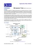
1 Custom Silicon solutions , Inc. 2009 1 Version , May 2009 cssCustom Silicon solutions , Inc. css555 Micropower Timer GENERAL PART DESCRIPTION The css555 is a micropower version of the popular 555 timer IC. It features an operating current under 5 A and a minimum supply voltage of , making it ideal for battery-operated applications. A six-decade programmable counter is included to allow generation of long timing delays. Configuration data for the counter is held in EEPROM to maintain the standard pin count of eight.
2 The analog circuits are temperature compensated to provide excellent stability over a wide ambient temperature range. A simple four-wire interface provides Read/Write access to the EEPROM. Key Features Pin Configuration Lowest power 555 timer (by > 10X)! Active mode current < 5 A Wide operating range Wide supply range: to Temperature range: -40 C to +85 C Internal 6 decade, programmable counter Settings = 1, 10, 102, 103, 104, 105 & 106 Multiplies delay time by up to 106 Figure 1 Delay times from microseconds to days Pin-for-pin compatible with 555 series timers Typical Application Circuit Monostable or Astable operation Extremely low transient switching current Break-Before-Make output driver Temperature stability per C Applications Portable & Battery-Powered Systems Precision Timing & Pulse Generation Figure 2 Ultra Long Period Delay Generation Single Cell Battery Applications Ordering Information
3 Ultra Low Power Timers Part Number Package DESCRIPTION Pulse Width Modulation css555 -ID 8 pin plastic DIP Low Cost, High Reliability Applications css555 -IS 8 pin plastic SOIC See page 9 for more details and options. Custom Silicon solutions Inc. 17951 Sky Park Circle, Suite F Irvine, CA 92614 (949) 797-9220 FAX: (949) 797-9225 GND TRIGGER OUTPUT RESET V+ DISCHARGE THRESHOLD CONTROL V 8 7 6 5 1 2 3 4 PDIP or SOIC css555 Long Period Delay Generator VDD RA RB Trigger Output Reset Operating conditions: RA = RB = , Internal counter = 106 (maximum) CT = 100pF, Delay = minutes Average power = W at VDD = 1 2 3 4 8765 css555 CT Custom Silicon solutions , Inc.
4 2009 2 Version , May 2009 css555 Micropower Timer Block Diagrams Standard 555 Timer Configuration (Std. Mode) (Programmable counter bypassed, Divider setting = 1) Figure 3 Extended Period Configuration (EP Mode) (Programmable counter enabled, Divider setting 10) Figure 4 EEPROM Bit Assignments Counter Configuration Divider Setting (Mult) Mode Control Bits Function xxxxx000 1 (Std. 555) xxxx0xxx Astable Mode ( Don t Care if Std. 555) xxxxx001 10 xxxx1xxx Monostable Mode ( Don t Care if Std.)
5 555) xxxxx010 100 xxx0xxxx Micro Power xxxxx011 1K xxx1xxxx Low Power xxxxx100 10K xx0xxxxx Standard voltage (Trip levels = & VDD) xxxxx101 100K xx1xxxxx Low voltage (Trip levels = 10% & 90% VDD) xxxxx110 1M Bit 6 Unused xxxxx111 1 (Std. 555) Bit 7 0 (Read Only) Table 1A Table 1B Note: For detailed programming information, see Application Note AN555-1 (CSS555_App_Note1_Serial_Interface) VDD _ + Comp _ + Comp R S Q Q Reset Flip Flop Control voltage Threshold VH VL R1 R2 R3 Reset VSS 1 56 4 8 Trigger 2 Enbl Clk Q Reset 6 Decade Counter Sel Clk Run Q Reset Trig Mode Control Mode Output Discharge 3 7 In0 In1 Out Sel 2.
6 1 Mux Configuration EEPROM _ + Comp _ + Comp R S Q Q Reset Flip Flop VDD Trigger Output Control voltage Threshold VH VL R1 R2 R3 Reset VSS 1 5 6 48 2 Discharge 3 7 R1+R2+R3 ~ 6 M For VDD > , VH = 2/3 x VDD, VL = 1/3 x VDD For VDD < , VH = x VDD, VL = x VDD Custom Silicon solutions , Inc. 2009 3 Version , May 2009 css555 Micropower Timer ELECTRICAL SPECIFICATIONS Absolute Maximum Ratings Supply voltage (VDD) 6V voltage at any Pin to VDD + Total Current into VDD Pin (Source) 50 mA Total Current out of GND Pin (Sink) 60 mA Storage Temperature Range -65 C to +140 C Note: Absolute maximum ratings indicate limits beyond which damage to the device may occur.
7 DC and AC electrical specifications are not ensured when operating the device at absolute maximum ratings. Electrical Characteristics Temperature = 25 C, Test Circuit #1, unless otherwise specified (If VDD < , Low voltage mode must be selected to provide adequate comparator input levels. EE Bit5 = 1) Parameter Symbol Conditions Min Typ Max Units Supply Range VDD Standard VDD (EE Bit 5 = 0) Low VDD (EE Bit 5 = 1) V V Supply Current (Power = Micro) (No DC load on OUTPUT pin, RL = ) IDD VDD = VDD = VDD = A A A Timing Accuracy (Micro power setting, EE Bit 4 = 0) (Monostable & Astable Modes) TAVDD RA(B) = 1M , CT = F VDD = VDD = VDD = % % % Timing Drift with Temperature (Monostable & Astable Modes) TDTEMP RA(B)
8 = 1M , CT = F VDD = VDD = VDD = 45 35 35 ppm/ C ppm/ C ppm/ C Timing Shift with Supply voltage (Monostable & Astable Modes) TSVDD RA(B) = 1M , CT = F VDD = VDD = VDD = %/V %/V %/V Maximum Oscillator Frequency fMAX RA,B = , CTI = 100 pF 1 MHz Control voltage VCTRL Standard VDD (EE Bit 5 = 0) Low VDD (EE Bit 5 = 1) 64 88 67 90 70 92 % V % V Trigger voltage VTRIG Standard VDD (EE Bit 5 = 0) Low VDD (EE Bit 5 = 1) 30 8 33 10 36 12 % V % V Reset voltage VRST x VDD x VDD x VDD V Output voltage (Timer Output Pin) VOL VDD = , ISINK = 1 mA VDD = , ISINK = 4 mA VDD = , ISINK = 10 mA V V V VOH VDD = , ISOURCE = 1 mA VDD = , ISOURCE = 4 mA VDD = , ISOURCE = 10 mA V V V Discharge Saturation voltage (Discharge Output Pin) VDIS VDD = , ISINK = mA VDD = , ISINK = 10 mA VDD = , ISINK = 25 mA V V V Input Current (Trigger, Reset & Threshold Inputs)
9 IIN VDD = VIN = to 10 pA Discharge Leakage Current IDIS VDD = 1 100 nA Output Rise & Fall Times tR, tF VDD = , CL = 10 pF 5 ns Input Capacitance CIN 10 pF Table 2 Custom Silicon solutions , Inc. 2009 4 Version , May 2009 css555 Micropower Timer Electrical Characteristics (cont) Temperature = -40 C to +85 C, Test Circuit #1, unless otherwise specified (If VDD < , Low voltage mode must be selected to provide adequate comparator input levels. EE Bit5 = 1) Parameter Symbol Conditions Min Typ Max Units Supply Range VDD Standard VDD (EE Bit 5 = 0) Low VDD (EE Bit 5 = 1) V V Supply Current (Power = Micro) (No DC load on OUTPUT pin, RL = ) IDD VDD = VDD = VDD = A A A Timing Accuracy (Micro power setting, EE Bit 4 = 0) (Monostable & Astable Modes) TAVDD RA(B) = 1M , CT = F VDD = VDD = VDD = % % % Timing Drift with Temperature (Monostable & Astable Modes) TDTEMP RA(B)
10 = 1M , CT = F VDD = VDD = VDD = 45 35 35 ppm/ C ppm/ C ppm/ C Timing Shift with Supply voltage (Monostable & Astable Modes) TSVDD RA(B) = 1M , CT = F VDD = VDD = VDD = %/V %/V %/V Maximum Oscillator Frequency fMAX RA,B = , CTI = 100 pF 1 MHz Control voltage VCTRL Standard VDD (EE Bit 5 = 0) Low VDD (EE Bit 5 = 1) 64 88 67 90 70 92 % V % V Trigger voltage VTRIG Standard VDD (EE Bit 5 = 0) Low VDD (EE Bit 5 = 1) 30 8 33 10 36 12 % V % V Reset voltage VRST x VDD x VDD x VDD V Output voltage (Timer Output Pin) VOL VDD = , ISINK = 1 mA VDD = , ISINK = 4 mA VDD = , ISINK = 10 mA V V V VOH VDD = , ISOURCE = 1 mA VDD = , ISOURCE = 4 mA VDD = , ISOURCE = 10 mA V V V Discharge Saturation voltage (Discharge Output Pin) VDIS VDD = , ISINK = mA VDD = , ISINK = 10 mA VDD = , ISINK = 25 mA V V V Input Current (Trigger, Reset & Threshold Inputs)