Transcription of Ground Sense Comparator - Rohm
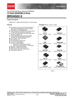
1 Product structure : Silicon monolithic integrated circuit This product has no designed protection against radioactive rays 1/ 53 2013 rohm Co., Ltd. All rights reserved. TSZ02201-0 RFR0G200200-1-2 TSZ22111 14 001 Ground Sense ComparatorBA8391G BA10393F BA10339 Series BA2903 Series BA2901 Series General Description General purpose BA8391G/BA10393F/BA10339xx and high reliability BA2903xxxx/BA2901xxx integrate one, two or four independent high gain voltage Comparator . Operating supply voltage range of BA8391G/BA1039 3F/BA2903xxxx/BA2901xxx is wide(2V to 36V). And can be used in a variety of applications because current consumption is small.
2 BA2903 Wxx is a low input offset voltage products.(2mV max) Features Operable with a Single Power Supply Wide Operating Supply Voltage Standard Pin A ssignments Input and Output are Ground Sense Operated Open Collector Wide Temperature Range Application General Use Current Monitor Battery Monitor Multi vibrator Key Specifications Operating Supply Voltage(Single Supply): BA8391G/BA10393F + to + BA2903xxxx/BA2901xxx + to + BA10339xx + to + Operating Supply Voltage(Split Supply): BA8391G/BA10393F to BA2903xxxx/BA2901xxx to BA10339xx to Temperature Range: BA8391G/BA10393F/ BA10339xx -40 C to +85 C BA2903 Sxxx/BA2901 Sxx -40 C to +105 C BA2903xxx/BA2901xx -40 C to +125 C Input Offset Voltage.
3 BA2903 Sxxx/BA2901 Sxx 7mV(Max) BA8391G/BA2903xxx/BA2901xx 7mV(Max) BA10393F/ BA10339xx 5mV(Max) BA2903 Wxx 2mV(Max) Packages W (Typ) x D(Typ) x H(Max) SSOP5 x x SOP8 x x SSOP-B8 x x MSOP8 x x SOP14 x x SSOP-B14 x x Selection Guide BA2903F BA2903FV BA2903 FVM BA2903SF BA2903 SFV BA2903 SFVM +125 C Maximum operating temperature Input Offset Voltage (Max) BA10339F BA10339FV BA10393F BA2901F BA2901FV BA2901SF BA2901 SFV +85 C +105 C General Purpose Dual Quad 5mV 5mV BA8391G Single 7mV High Reliability Dual 7m Quad 7mV 2mV BA2903WF BA2903 WFV Datasheet Datasheet TSZ02201-0 RFR0G200200-1-2 2013 rohm Co.
4 , Ltd. All rights reserved. 2/53 TSZ22111 15 001 BA8391G BA10393F BA10339 Series BA2903 Series BA2901 Series 34215-+OUT-IN+INVEEVCCS implified Schematic Pin Configuration BA8391G : SSOP5 Pin No. Pin Name 1 -IN 2 VEE 3 +IN 4 OUT 5 VCC BA10393F, BA2903SF, BA2903F, BA2903WF : SOP8 BA2903 SFV, BA2903FV, BA2903 WFV : SSOP-B8 BA2903 SFVM,BA2903 FVM : MSOP8 Pin No. Pin Name 1 OUT1 2 -IN1 3 +IN1 4 VEE 5 +IN2 6 -IN2 7 OUT2 8 VCC Figure 1. Simplified Schematic (one channel only) -IN VCC +IN VEE OUT -++ -CH1CH281234567 OUT1-IN1+IN1 VEEVCCOUT2-IN2+IN2 Datasheet TSZ02201-0 RFR0G200200-1-2 2013 rohm Co.
5 , Ltd. All rights reserved. 3/53 TSZ22111 15 001 BA8391G BA10393F BA10339 Series BA2903 Series BA2901 Series Pin Configuration - continued BA10339F, BA2901SF, BA2901F : SOP14 BA10339FV, BA2901 SFV, BA2901FV : SSOP-B14 Package SSOP5 SOP8 SSOP-B8 MSOP8 SOP14 SSOP-B14 BA8391G BA10393F BA2903SF BA2903F BA2903WF BA2903 SFV BA2903FV BA2903 WFV BA2903 SFVM BA2903 FVM BA10339F BA2901SF BA2901F BA10339FV BA2901 SFV BA2901FV Ordering Information B A x x x x x x x x - x x Part Number BA8391 BA10393xx BA10339xx BA2901xx BA2901 Sxx BA2903xx BA2903 Sxx BA2903 Wxx Package G : SSOP5 F.
6 SOP8 SOP14 FV : SSOP-B8 SSOP-B14 FVM : MSOP8 Packaging and forming specification E2: Embossed tape and reel (SOP8/SOP14/SSOP-B8/SSOP-B14) TR: Embossed tape and reel (SSOP5/MSOP8) Pin No. Pin Name 1 OUT2 2 OUT1 3 VCC 4 -IN1 5 +IN1 6 -IN2 7 +IN2 8 -IN3 9 +IN3 10 -IN4 11 +IN4 12 VEE 13 OUT4 14 OUT3 OUT2 OUT1 VCC-IN1+IN1-IN2+IN2 OUT3 OUT4 VEE+IN4-IN4+IN3-IN3 1234567891011121314CH1CH3CH2 CH4 Datasheet TSZ02201-0 RFR0G200200-1-2 2013 rohm Co., Ltd. All rights reserved. 4/53 TSZ22111 15 001 BA8391G BA10393F BA10339 Series BA2903 Series BA2901 Series Line-up Operating Temperature Range Input Offset Voltage (Max) Supply Current (Typ)
7 Package Orderable Part Number -40 C to +85 C 7mV SSOP5 Reel of 3000 BA8391G-TR 5mV SOP8 Reel of 2500 BA10393F-E2 SOP14 Reel of 2500 BA10339F-E2 SSOP-B14 Reel of 2500 BA10339FV-E2 -40 C to +105 C 7mV SOP8 Reel of 2500 BA2903SF-E2 SSOP-B8 Reel of 2500 BA2903 SFV-E2 MSOP8 Reel of 3000 BA2903 SFVM-TR SOP14 Reel of 2500 BA2901SF-E2 SSOP-B14 Reel of 2500 BA2901 SFV-E2 -40 C to +125 C SOP8 Reel of 2500 BA2903F-E2 SSOP-B8 Reel of 2500 BA2903FV-E2 MSOP8 Reel of 3000 BA2903 FVM-TR 2mV SOP8 Reel of 2500 BA2903WF-E2 SSOP-B8 Reel of 2500 BA2903 WFV-E2 7mV SOP14 Reel of 2500 BA2901F-E2 SSOP-B14 Reel of 2500 BA2901FV-E2 Absolute Maximum Ratings (Ta=25 C) Parameter Symbol Rating Unit BA8391G Supply Voltage VCC-VEE +36 V Power Dissipation PD SSOP5 (Note1,2) W Differential Input Voltage (Note 3) VID +36 V Input Common-mode Voltage Range VICM ( ) to (VEE+36) V Input Current (Note 4) II -10 mA Operating Supply Voltage Vopr + to + ( to ) V Operating Temperature Range Topr -40 to +85 C Storage Temperature Range Tstg -55 to +150 C Maximum Junction Temperature Tjmax +150 C (Note 1) To use at temperature above TA 25 C reduce (Note 2) Mounted on a FR4 glass epoxy PCB(70mm 70mm ).
8 (Note 3) The voltage difference between inverting input and non-inverting input is the differential input voltage. Then input terminal voltage is set to more than VEE. (Note 4) Excessive input current will flow if a differential input voltage in excess of approximately is applied between the input unless some limiting resistance is used. Caution: Operating the IC over the absolute maximum ratings may damage the IC. The damage can either be a short circuit between pins or an open circuit between pins and the internal circuitry. Therefore, it is important to consider circuit protection measures, such as adding a fuse, in case the IC is operated over the absolute maximum ratings.
9 Datasheet TSZ02201-0 RFR0G200200-1-2 2013 rohm Co., Ltd. All rights reserved. 5/53 TSZ22111 15 001 BA8391G BA10393F BA10339 Series BA2903 Series BA2901 Series Absolute Maximum Ratings - continued Parameter Symbol Rating Unit BA10393F BA10339xx Supply Voltage VCC-VEE +36 V Power Dissipation PD SOP8 (Note 5,8) - W SOP14 - (Note 6,8) SSOP-B14 - (Note 7,8) Differential Input Voltage(Note 9) VID (VEE to VCC) V Input Common-mode Voltage Range VICM ( ) to VCC V Input Current(Note 10) II -10 mA Operating Supply Voltage Vopr + to + ( to ) + to + ( to ) V Operating Temperature Range Topr -40 to +85 C Storage Temperature Range Tstg -55 to +125 C Maximum Junction Temperature Tjmax +125 C (Note 5) To use at temperature above TA 25 C reduce (Note 6) To use at temperature above TA 25 C reduce (Note 7) To use at temperature above TA 25 C reduce (Note 8) Mounted on a FR4 glass epoxy PCB(70mm 70mm ).
10 (Note 9) The voltage difference between inverting input and non-inverting input is the differential input voltage. Then input terminal voltage is set to more than VEE. (Note 10) Excessive input current will flow if a differential input voltage in excess of approximately is applied between the input unless some limiting resistance is used. Caution: Operating the IC over the absolute maximum ratings may damage the IC. The damage can either be a short circuit between pins or an open circuit between pins and the internal circuitry. Therefore, it is important to consider circuit protection measures, such as adding a fuse, in case the IC is operated over the absolute maximum ratings.