Transcription of High-Brightness LED Matrix Manager for …
1 Product Sample & Technical Tools & Support &. Folder Buy Documents Software Community TPS92661-Q1. SLUSBU2A SEPTEMBER 2014 REVISED FEBRUARY 2016. High-Brightness LED Matrix Manager for Automotive Headlight Systems 1 Features The TPS92661 device includes a 12-switch series array for bypassing individual LEDs in the string and . 1 12 Series LED Bypass Switches a serial communication interface for control and Multi-Drop UART Communication Interface management by a master microcontroller. Programmable 10-bit PWM Dimming An on-board charge pump rail that can float up to Individual Turn-on and Turn-off Times 67 V above GND provides the LED bypass switch Inherent Phase Shift Capability gate low on-resistance (RDS(on)) of the bypass switch minimizes conduction loss and power Device-to-Device Synchronization dissipation.
2 LED Open/Short Detection and Protection The TPS92661 device contains a multi-drop universal Fault Reporting asynchronous receiver transmitter (UART) for serial AEC-Q100 Grade 1 communication. The turn-on and turn-off times are Thermally Enhanced Package programmable for each individual LED in the string. The PWM frequency is adjustable via an internal 48-pin, TQFP, Exposed Pad Package register and multiple devices can be synchronized to the same frequency and phase. 2 Applications The TPS92661 device features open LED protection Automotive headlight systems as well as open and short LED fault reporting via the High-Brightness LED Matrix Systems serial interface. The TQFP package features a feed-through topology 3 Description to enable easy routing of signals on single-layer The TPS92661 device is a compact, highly-integrated metal core LED load boards.
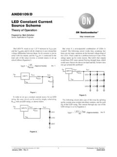
3 Solution for shunt FET dimming for large arrays of High-Brightness LEDs in applications such as Device Information(1). automotive headlights. PART NUMBER PACKAGE BODY SIZE (NOM). TPS92661-Q1 PHP (48) mm mm (1) For all available packages, see the orderable addendum at the end of the data sheet. Simplified System Schematic Driver Module LED Module VBAT Boost Voltage DC Voltage Rail Buck Current Regulator Regulator LED12 LED1. TPS92661. n Channels Buck Current 5V LED Matrix Buck Manager 1. or Supply Regulators 5-V V and Auxiliary Return n Channels Matrix Voltage Cable Regulators Manager C Buck Current Regulator LED12 LED1. TPS92661. CAN Rx LED Matrix CAN. Cable Manager n Xcvr Bus Tx 1. An IMPORTANT NOTICE at the end of this data sheet addresses availability, warranty, changes, use in safety-critical applications, intellectual property matters and other important disclaimers.
4 PRODUCTION DATA. TPS92661-Q1. SLUSBU2A SEPTEMBER 2014 REVISED FEBRUARY 2016 Table of Contents 1 Features .. 1 8 Application and Implementation .. 38. 2 Applications .. 1 Applications 38. 3 Description .. 1 Design Examples .. 38. 4 Revision 2 9 Power Supply 40. 5 Pin Configuration and Functions .. 3 General Recommendations .. 40. Internal 40. 6 4. Power Up and 41. Absolute Maximum Ratings .. 4. VIN Power 41. ESD 5. Initialization Set-Up .. 41. Recommended Operating 5. Thermal Information .. 5 10 43. Electrical 6 Layout Guidelines .. 43. Typical Characteristics .. 7 Layout Example .. 43. 7 Detailed Description .. 9 11 Device and Documentation Support .. 44. Overview .. 9 Trademarks .. 44. Functional Block Diagram .. 10 Electrostatic Discharge Caution .. 44. Feature 10 Export Control 44.
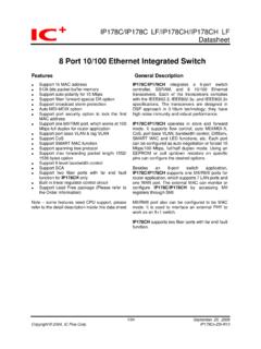
5 Device Functional 20 Glossary .. 44. 31 12 Mechanical, Packaging, and Orderable Register 35 Information .. 45. 4 Revision History NOTE: Page numbers for previous revisions may differ from page numbers in the current version. Changes from Original (September 2014) to Revision A Page Added output current range specifications in Recommended Operating Conditions table .. 5. Added updated text to the section UART Communications Reset to indicate that a communications reset should only be sent when the device is not transmitting 23. 2 Submit Documentation Feedback Copyright 2014 2016, Texas Instruments Incorporated Product Folder Links: TPS92661-Q1. TPS92661-Q1. SLUSBU2A SEPTEMBER 2014 REVISED FEBRUARY 2016. 5 Pin Configuration and Functions PHP Package 48-Pin TQFP. Top View LED12. LED11.
6 LED10. LED9. LED8. LED7. LED6. LED5. LED4. LED3. LED2. LED1. 48 47 46 45 44 43 42 41 40 39 38 37. CPP 1 36 LED0. NC 2 35 NC. GND 3 34 GND. EN 4 33 EN. GND 5 32 GND. SYNC 6 31 SYNC. Thermal Pad GND 7 30 GND. CLK 8 29 CLK. GND 9 28 GND. TX 10 27 TX. GND 11 26 GND. RX 12 25 RX. 13 14 15 16 17 18 19 20 21 22 23 24. VCC. VIN. ADR1. ADR2. NC. NC. NC. NC. NC. ADR0. VIN. GND. Pin Functions PIN. I/O DESCRIPTION. NAME NO. ADR0 22 I Least significant bit (LSB) of device address. Connect to VIN or GND. ADR1 15 I Second bit of device address. Connect to VIN or GND. ADR2 16 I Most significant bit (MSB) of device address. Connect to VIN or GND. 8 System clock. This clock is provided externally (by the microcontroller unit or an external CLK I. 29 oscillator) and is the primary clock for the device.
7 Charge pump output. Bypass with a ceramic capacitor with a minimum value of F to CPP 1 I. LED12. 4 Enable pins. The device is active when EN is high or in reset when EN is low. Connect to EN I. 33 microcontroller unit output or tie to VCC or VIN for enable at power-up. 3, 5, 7, 9, 11, GND 24, 26, 28, Device system ground. All pins MUST be connected for proper operation. 30, 32, 34. LED0 36 O Connect to cathode of LED1. LED1 37 O Connect to anode of LED1 and cathode of LED2. LED2 38 O Connect to anode of LED2 and cathode of LED3. Copyright 2014 2016, Texas Instruments Incorporated Submit Documentation Feedback 3. Product Folder Links: TPS92661-Q1. TPS92661-Q1. SLUSBU2A SEPTEMBER 2014 REVISED FEBRUARY 2016 Pin Functions (continued). PIN. I/O DESCRIPTION. NAME NO. LED3 39 O Connect to anode of LED3 and cathode of LED4.
8 LED4 40 O Connect to anode of LED4 and cathode of LED5. LED5 41 O Connect to anode of LED5 and cathode of LED6. LED6 42 O Connect to anode of LED6 and cathode of LED7. LED7 43 O Connect to anode of LED7 and cathode of LED8. LED8 44 O Connect to anode of LED8 and cathode of LED9. LED9 45 O Connect to anode of LED9 and cathode of LED10. LED10 46 O Connect to anode of LED10 and cathode of LED11. LED11 47 O Connect to anode of LED11 and cathode of LED12. LED12 48 O Connect to anode of LED12. 2, 17, 18, 19, NC No connection. 20, 21, 35. 12 Received data pins. Connect one RX pin of first device to microcontroller unit TX output and RX I/O use second pin to connect to a RX pin of the second device. All other devices use both pins 25 to route the RX line through each device. 6 Synchronization pins.
9 Allows synchronization of multiple TPS92661 devices on the same network. May be driven by the microcontroller unit, or one TPS92661 device may be SYNC I/O. 31 programmed via the serial interface to provide this pulse. Only one device should drive this signal. May be left unconnected if not used. 10 Transmitted data pins. Connect one TX pin of first device to microcontroller unit RX input and TX I/O use second pin to connect to a TX pin of the second device. All other devices use both pins 27 to route the TX line through each device. This pin requires a 100k pull-up resistor. Output of the on-board LDO. This pin requires a ceramic output capacitor with a value VCC 13 O. of F or greater. Tie to the VIN pin for 5-V microcontroller unit systems. 14 5-V power supply input for device. Bypass with a ceramic capacitor with a minimum value of VIN I.
10 23 F. Thermal Pad - Connect to system GND. 6 Specifications Absolute Maximum Ratings (1) (2). Over operating free-air temperature range (unless otherwise noted). MIN MAX UNIT. VIN, VCC to GND 7. CPP to GND 67. CPP to LED12 7. Input voltage V. LEDx to GND 60. LEDx to LED(x-1) 7. SYNC, EN, CLK, TX, RX, ADR0-2 to GND 7. Storage temperature range, Tstg 40 150 C. (1) Stresses beyond those listed under Absolute Maximum Ratings may cause permanent damage to the device. These are stress ratings only, which do not imply functional operation of the device at these or any other conditions beyond those indicated under Recommended Operating Conditions. Exposure to absolute-maximum-rated conditions for extended periods may affect device reliability. (2) If Military/Aerospace specified devices are required, contact the Texas Instruments Sales/Office/Distributors for availability and specifications.