Transcription of High-Efficiency Controller for Boost, SEPIC, and Flyback ...
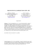
1 LM3481 VINISENCOMPFBAGNDUVLOVCCDRPGNDFA/SYNC/SD ++VIN = 5 VVOUT = 12VR7121 k:R8121 k:CC82 nFC8 390 k:RF220 k:RF1169 k:RSEN 20 m:CSEN1 nF1 PFCIN1, CIN2 150 PHIOUT = , COUT2 150 PFC9D1Q1 ProductFolderSample &BuyTechnicalDocumentsTools &SoftwareSupport &CommunityAn IMPORTANTNOTICEat the end of this datasheetaddressesavailability,warranty, changes,use in safety-criticalapplications,intellectual propertymattersand ,LM3481-Q1 SNVS346F NOVEMBER2007 REVISEDNOVEMBER2014LM3481/ -Q1 high -EfficiencyControllerfor Boost, SEPICand FlybackDC-DCConverters11 Features1 LM3481 QMMare Automotive-GradeProductsThatare AEC-Q100 Grade1 Qualified( 40 C to+125 C OperatingJunctionTemperature) 10-LeadVSSOPP ackage InternalPush-PullDriverWith1-A PeakCurrentCapability CurrentLimitand ThermalShutdown FrequencyCompensationOptimizedWithaCapac itorand a Resistor InternalSoftstart CurrentModeOperation AdjustableUndervoltageLockoutWithHystere sis PulseSkippingat LightLoads Key Specifications WideSupplyVoltageRangeof to 48 V 100-kHzto 1-MHzAdjustableandSynchronizableClockFre quency (OverTemperature)InternalReference 10- A ShutdownCurrent(OverTemperature)
2 Createa CustomDesignUsingthe LM3481withthe WEBENCHP owerDesigner2 Applications AutomotiveStart-StopApplications AutomotiveADASD riverInformation One Cell/TwoCell Li-ionBatteryPoweredPortableBluetoothAud ioSystems Notebooks,PDAs,DigitalCameras,and OtherPortableApplications OfflinePowerSupplies Set-TopBoxes Boostfor AudioAmplifiers3 DescriptionTheLM3481deviceis a versatileLow-SideN-FEThigh-performanceco ntrollerfor deviceis designedfor use in Boost, SEPICandFlybackconvertersandtopolo giesrequiringa low-sideFETas the LM3481devicecan be operatedat very high the LM3481devicecan be adjustedtoany valuebetween100kHzand1 MHzby usingasingleexternalresistoror by synchronizingit to transientresponsein additionto can beprogrammedwith a built-inprotectionfeaturessuchas thermalshutdown,short-circuitprotectiona nd totalsupplycurrentto 5 A inrushcurrentat designand,ifneededfor specificapplications,can be increasedusinga (1)PARTNUMBERPACKAGEBODYSIZE(NOM)LM3481 VSSOP(10) (1) For all availablepackages,see the orderableaddendumatthe end of the LM3481 Typical5V to 12V BoostConverterApplication2LM3481,LM3481- Q1 SNVS346F NOVEMBER2007.
3 LM3481LM3481-Q1 SubmitDocumentationFeedbackCopyright 2007 2014,TexasInstrumentsIncorporatedTableof Contents1 Pin Configurationand Applicationand Deviceand Mechanical,Packaging,and RevisionHistoryChangesfromRevisionE (April2012)to RevisionFPage AddedPin Configurationand Functionssection,HandlingRatingtable,Fea tureDescriptionsection,DeviceFunctionalM odes,Applicationand Implementationsection,PowerSupplyRecomme ndationssection,Layoutsection,Deviceand DocumentationSupportsection,andMechanica l,Packaging,and , NOVEMBER2007 REVISEDNOVEMBER2014 ProductFolderLinks:LM3481LM3481-Q1 SubmitDocumentationFeedbackCopyright 2007 2014,TexasInstrumentsIncorporated5 Pin Configurationand Functions10-PinVSSOPP ackageTop ViewPin Voltagegeneratedacrossan externalsenseresistoris fed into this A resistordividerfromVINto groundis connectedto the UVLOpin.
4 Theratioof theseresistancesdeterminethe inputvoltagewhichallowsswitchingand the A resistorand capacitorcombinationconnectedto this pin providescompensationfor the Invertinginputof the Internalbias connectedto PGNDat a ,synchronization,and shutdownpin. A resistorconnectedfromthis pin to groundsets the externalclocksignalat this pin will synchronizethe controllertothe frequencyof the high levelon this pin for 30 s will turn the deviceoff and the devicewill thendraw5 A fromthe connectedto AGNDat a of the IC. The gateof the externalMOSFET shouldbe connectedto this A bypasscapacitormustbe connectedfromthis pin to not bias ,LM3481-Q1 SNVS346F NOVEMBER2007 :LM3481LM3481-Q1 SubmitDocumentationFeedbackCopyright 2007 2014,TexasInstrumentsIncorporated(1)Abso luteMaximumRatingsare limitsbeyondwhichdamageto the devicemay whichthe deviceis intendedto be functional,but doesnot ensuredspecificationsand test conditions,see theElectricalCharacteristics.
5 The ensuredspecificationsapplyonly for the test conditions.(2)Part is MSL1-260 Cqualified6 (unlessotherwisenoted)(1)MINMAXUNITVINPi n Voltage Voltage Voltage Voltage Voltage Voltage Voltage Voltage 400600mVPeakDriverOutputCurrent1 APowerDissipationInternallyLimitedJuncti onTemperature150 CLeadTemperature(onlyappliestooperatingc onditions)DGSP ackage220 CPeakBodyTemperature(2)260 C(1)JEDEC documentJEP155statesthat 500-VHBM allowssafe manufacturingwith a standardESDcontrolprocess.(2)JEDEC documentJEP157statesthat 250-VCDM allowssafe manufacturingwith a :LM3481 MINMAXUNITTstgStoragetemperaturerange 65150 CV(ESD)ElectrostaticdischargeHumanbodymo del(HBM),per ANSI/ESDA/JEDECJS-001,allpins(1) 2000+2000 VChargeddevicemodel(CDM),per JEDEC specificationJESD22-C101,all pins(2) 750+750(1)AECQ100-002indicatesHBMstressi ngis donein accordancewith the ANSI/ :LM3481-Q1 MINMAXUNITTstgStoragetemperaturerange 65150 CV(ESD)ElectrostaticdischargeHumanbodymo del(HBM),per AECQ100-002(1) 2000+2000 VChargeddevicemodel(CDM),perAECQ100-011 Cornerpins (1, 5, 6,and 10) 750+750 Otherpins 750+ 40125 CSwitchingFrequencyRange1001kHz/MHz5LM34 81, NOVEMBER2007 REVISEDNOVEMBER2014 ProductFolderLinks.
6 LM3481LM3481-Q1 SubmitDocumentationFeedbackCopyright 2007 2014,TexasInstrumentsIncorporated(1)For moreinformationabouttraditionaland new thermalmetrics,see theIC PackageThermalMetricsapplicationreport, (1)LM3481 UNITVSSOP10 PINSR C/WR JC(top)Junction-to-case(top) JC(bot)Junction-to-case(bottom)thermalre sistance-(1)The drivepin voltage,VDR, is equalto the inputvoltagewheninputvoltageis less than6 V. VDRis equalto 6 V whenthe inputvoltageis greaterthanor equalto 6 V.(2)For this test, the FA/SYNC/SDPin is pulledto groundusinga 40-k 12 V, RFA= 40 k , TJ= 25 C, V, VIN 48 V, VIN 48 V, 40 C TJ 125 VLINEF eedbackVoltageLine VIN 48 VLOADO utputVoltageLoadRegulationIEAOS ource/Sink , 40 C TJ 125 AEnabled, 40 C TJ 125 CurrentSinkVFB= 0V640 AVCOMPVFB= 40 k 475kHzRFA= 40 k , 40 C TJ 125 C406550 Vsync-HIThresholdfor SynchronizationonFA/ SynchronizationonFA/ (ON)DriverSwitchOn Resistance(top)IDR= ,VIN= 5 V4 RDS2(ON)DriverSwitchOn Resistance(bottom)IDR= VDR (max)MaximumDriveVoltageSwing(1)VIN< 6 VVINVVIN 6V6 DmaxMaximumDutyCycleRFA=40 k 81%85%tmin(on)MinimumOn Time250363nsworstcaseovertemperature571n sISUPPLYS upplyCurrent(switching)See(2) (2), 40 C TJ 125 ,LM3481-Q1 SNVS346F NOVEMBER2007.
7 LM3481LM3481-Q1 SubmitDocumentationFeedbackCopyright 2007 2014,TexasInstrumentsIncorporatedElectri calCharacteristics(continued)VIN= 12 V, RFA= 40 k , TJ= 25 C, (3)For this test, the FA/SYNC/SDPin is pulledto 3 V usinga 40-k resistor.(4)The overvoltageprotectionis specifiedwith respectto the is becausethe overvoltagethresholdcan be calculatedby addingthe feedbackvoltage(VFB) to the overvoltageprotectionspecification.(5)Th e FA/SYNC/SDpin shouldbe pulledto VINthrougha resistorto turn the regulatoroff. The voltageon the FA/SYNC/SDpin mustbeabovethe max limit for the Output= Highlongerthan30 s to keepthe regulatoroff and mustbe belowthe minimumlimit for Output=Low to keepthe ShutdownModeVFA/SYNC/SD= 3 V(3), VIN= 12 V9 AVFA/SYNC/SD= 3 V(3), VIN= 12 V, 40 C TJ 125 C15 VFA/SYNC/SD= 3 V(3), VIN= 5 V5 VFA/SYNC/SD= 3 V(3), VIN= 5 V, 40 C TJ 125 C10 VSENSEC urrentSenseThresholdVoltage160mV 40 C TJ 125 C100190 VSCOverLoadCurrentLimitSenseVoltage220mV 40 C TJ 125 C157275 VSLI nternalCompensationRampVoltage90mVVOVPO utputOver-voltageProtection(withrespectt o feedbackvoltage)(4)VCOMP= V85mVVCOMP= V, 40 C TJ 125 C26135 VOVP(HYS)
8 OutputOver-VoltageProtectionHysteresisVC OMP= V70mVVCOMP= V, 40 C TJ 125 C28106 GmErrorAmplifierTransconductanceVCOMP= V450 mhoVCOMP= V, 40 C TJ 125 C216690 AVOLE rrorAmplifierVoltageGainVCOMP= V, IEAO= 100 A(Source/Sink)60V/VVCOMP= V, IEAO= 100 A(Source/Sink), 40 C TJ 125 C3566 IEAOE rrorAmplifierOutputCurrent(Source/Sink)S ource,VCOMP= V, VFB= V640 ASource,VCOMP= V, VFB= V, 40 C TJ 125 C475837 Sink,VCOMP= V, VFB= V65 ASink,VCOMP= V, VFB= V, 40 C TJ 125 C31100 VEAOE rrorAmplifierOutputVoltageSwingUpperLimi t:VFB= 0 V, :VFB= 0 V, COMPPinFloating, 40 C TJ 125 :VFB= :VFB= V, 40 C TJ 125 V, COMPPin RiseTimeCgs = 3000pf, VDR= 0 V to 3 V25nstfDrivePin Fall TimeCgs = 3000pf, VDR= 3 V to 0 V25nsVSDS hutdownsignalthreshold(5)FA/SYNC/SDpinOu tput= high (Shutdown) high (Shutdown), 40 C TJ 125 Low (Enable) Low (Enable), 40 C TJ 125 , NOVEMBER2007 REVISEDNOVEMBER2014 ProductFolderLinks:LM3481LM3481-Q1 SubmitDocumentationFeedbackCopyright 2007 2014,TexasInstrumentsIncorporatedElectri calCharacteristics(continued)VIN= 12 V, RFA= 40 k , TJ= 25 C, CurrentFA/SYNC/SDpinVSD= 5 V 1 AVSD= 0 V20 TSDT hermalShutdown165 CTshThermalShutdownHysteresis10 C8LM3481,LM3481-Q1 SNVS346F NOVEMBER2007 :LM3481LM3481-Q1 SubmitDocumentationFeedbackCopyright 2007 2014, ,VIN= 12 V, TJ= 25 CompPin Voltagevs.
9 LoadCurrentFigure4. SwitchingFrequencyvs. RFAF igure5. Efficiencyvs. LoadCurrent( VINand 12 VOUT)Figure6. Efficiencyvs. LoadCurrent(5 VINand 12 VOUT)Figure7. Efficiencyvs. LoadCurrent(9 VINand 12 VOUT)Figure8. Frequencyvs. Temperature9LM3481, NOVEMBER2007 REVISEDNOVEMBER2014 ProductFolderLinks:LM3481LM3481-Q1 SubmitDocumentationFeedbackCopyright 2007 2014,TexasInstrumentsIncorporatedTypical Characteristics(continued)Unlessotherwis especified,VIN= 12 V, TJ= 25 COMPPin SourceCurrentvs. TemperatureFigure10. ISupplyvs. InputVoltage(Nonswitching)Figure11. ISupplyvs. InputVoltage(Switching)Figure12. ShutdownThresholdHysteresisvs. TemperatureFigure13. DriveVoltagevs. InputVoltageFigure14. ShortCircuitProtectionvs. VIN10LM3481,LM3481-Q1 SNVS346F NOVEMBER2007 :LM3481LM3481-Q1 SubmitDocumentationFeedbackCopyright 2007 2014,TexasInstrumentsIncorporatedTypical Characteristics(continued)Unlessotherwis especified,VIN= 12 V, TJ= 25 CurrentSenseThresholdvs.
10 InputVoltageFigure16. CompensationRampAmplitudevs. InputVoltageFigure17. MinimumOn-Timevs. TemperaturePWM ComparatorOscillator Sets the RS LatchPWM Comparator resets the RS latchBlank-Out prevents false reset+_VSLTmin (on) Blank-Out time11LM3481, NOVEMBER2007 REVISEDNOVEMBER2014 ProductFolderLinks:LM3481LM3481-Q1 SubmitDocumentationFeedbackCopyright 2007 2014,TexasInstrumentsIncorporated7 LM3481deviceusesa fixedfrequency,PulseWidthModulated(PWM), typicalapplicationcircuit,the peakcurrentthroughthe externalMOSFETis sensedthroughan voltageacrossthis resistoris fed into the ISENpin. This voltageis thenlevelshiftedand fed into thepositiveinputof the outputvoltageis also sensedthroughan externalfeedbackresistordividernetworkan d fed into the erroramplifier(EA)negativeinput(feedback pin, FB).