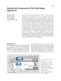
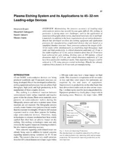
Transcription of History and Future of Hitachi's Plasma Etching System
1 History and Future of hitachi s Plasma Etching System 198 History and Future of hitachi s Plasma Etching SystemHiromichi EnamiYoshifumi OgawaMasaru IzawaTakaaki SaitoINTRODUCTIONMANUFACTURING semiconductors such as ULSI (ultra-large-scale integration) chips requires creating multiple levels of patterns on a silicon substrate to form active devices such as transistors, memory elements and wire connections. Each layer of the pattern is formed by a series of steps such as deposition, lithography, Etching , and impurity diffusion. In this process, the role of Etching is to create the actual pattern by transferring the organic resist pattern formed by lithography to the material(s) below.
2 Technical challenges include the etch rate, selectivity, and dimension control. Performance requirements have become stricter with each successive device number of etch process steps is increasing with every generation. Typical devices currently require between 30 and 50 etch steps with minimum processing dimensions in the range of tens of nanometers and more than 10 wire connection layers. Meanwhile, the adoption of new metal materials and three dimensional device structures has resulted in a higher and more exacting level of performance. In the early 2000s, equipment productivity emerged as a key requirement because large memory foundries were constructed during the wafer size transition to 300 mm.
3 As shown in Fig. 1, equipment suppliers are now required to provide solutions to the productivity improvement challenges that customers are facing.(1) History OF ETCH EQUIPMENT DEVELOPMENTFull-scale development of hitachi Etching equipment started in 1981 at hitachi , Ltd. s Kasado-works. This was a collaboration between internal semiconductor development and production sites including the Central Research Laboratory, Device Development Center, and Semiconductor & Integrated Circuit Division. It initially led to the development of OVERVIEW: hitachi s Etching equipment business has been firmly established since it began research into magneto-microwave plasmas in 1983.
4 This business has continued to expand by developing and implementing superior technologies such as on-board post-etch processing stations and electrostatic chucks. Market requirements have continued to change with each increase in wafer size (200 mm to 300 mm in 2000), the shift in HVM device manufacturing from Japan to Asia, and the continuous reduction in feature sizes predicted by Moore s Law. hitachi has continued to grow this business by anticipating changes in the market and creating competitive products. For example, hitachi has been in the forefront of the creation of additional functions that can increase the production efficiency of our etchers.
5 These functionality enhancements have been implemented by some of our customers ahead of the general market resulting in substantial manufacturing advantages. hitachi will continue to expand this product line in order to meet the requirements for Future semiconductor devices which include reducing the impact on the reductions of about 12 14% per yearTimeChip cost per function (log)Increased wafer diameterImproved yieldIncreasing productivity25 30% cost reduction per yearPresentTa rgeted chip costOther productivity improvementsFig. 1 Tactics for Improving aim is to reduce the functional cost of chips by 25 to 30% per year by reducing feature size, improving yield, and increasing productivity.
6 The measures for improving productivity are the most Review Vol. 60 (2011), No. 5 199 batch-type (RE-504) and single-wafer-type (R-206A) parallel plate RIE (reactive ion Etching ) systems which were the mainstream technologies at the time. This equipment, however, was only used within the company since the performance did not surpass that of competing equipment. Meanwhile, research aimed at supporting a m semiconductor processes, and developing etch equipment for submicron processes started in 1983. The research group developed an Etching method characterized by the formation of a high-density Plasma (ECR) using the magneto-microwave technique with independent control of ion acceleration to the wafer using a different high-frequency power source.
7 This ECR System gave a superior etch rate to competing equipment as well as better etch accuracy for policide gate processing. It was first adopted for 1-M DRAM (dynamic random access memory) production and was introduced to the market as the M-206A single-wafer etcher [see Fig. 2(a)]. In the m metal wiring process, a triple-layer structure using a barrier-metal was adopted to prevent aluminum film migration. The ECR System also had significant advantages when used for vertical Etching of this structure. This result led to the development of the M-308AT single-wafer Etching System which was sold with an additional post-etch processing chamber integrated in vacuum wafer transfer for improved corrosion resistance [see Fig.]
8 2(b)].Since this time, hitachi has improved its product development methods to better reflect customer needs while also incorporating new technologies into the equipment based on these two original models. Examples include:(1) Electrostatic chuck (see Fig. 3)This technology improved wafer cooling efficiency significantly by using electrostatic chucking to fix the wafer to the electrode. hitachi was five years ahead of its competitors in providing a solution which address the potential of charge-up damage.(2) Time modulation biasThis technology can repeat oscillation in the high-frequency bias for ion acceleration on a time scale of milliseconds.
9 It has been effective for controlling profile and selectivity and has been the subject of continuous improvement.(3) Low-temperature etchingLow-temperature technology developed at the Central Research Laboratory was further improved and adapted for use in mass production. It is currently used for deep hole and trench 3 Overview of Electrostatic Chuck and Graphic of Reactive Chamber with Electrostatic electrostatic chuck mechanism played an important role in wafer temperature control but was difficult to install on equipment due to lifetime and damage issues. Despite this, hitachi was able to develop and commercialize the technology within a year by collaborating with customers and parts 4 Evolution of Magneto-microwave Plasma Use in Silicon Etching quartz bell-jar design was adopted for the M-206A and M-318EX and the applied cavity resonance design has been used since the M-511A to improve uniformity on larger wafers.
10 Further improvements were added to improve uniformity and 2 Equipment Developed through Special Research beta tool incorporating a magneto-microwave Plasma source was installed at the Device Development Center in late design improvements and process evaluation, the unit was re-installed as the first upgraded M-206A in late 1985 (a). The M-308AT was introduced to the market in 1987. Based on the M-206A, it also incorporated further upgrades and an on-board post-etch processing module (b).(a) M-206A(b) M-308 ATModelPlasma sourceBias frequencyGas introduction Exhaust flowTemperaturecontrol methodBias control GHz + Auto tuning2 MHzM-511A800 kHzM-712AM-712 XTM-8190XT400 kHzSide wallAsymmetrySingle zone2 zoneCavity resonance typeQuartz bell-jar3 zone(with heater)SymmetryContinuousSPContinuous/ti me modulationNew SPNew typeSP: shower plateHistory and Future of hitachi s Plasma Etching System 200 (4) EMCP (electromagnetically coupled Plasma )This uses a unique functional shield technology and achieves good processing characteristics for Etching non-volatile materials.