Transcription of ICL8038
1 1 SemiconductorCAUTION: These devices are sensitive to electrostatic discharge; follow proper IC Handling Harris Corporation 1998 ICL8038 Precision Waveform Generator/VoltageControlled OscillatorThe ICL8038 waveform generator is a monolithic integratedcircuit capable of producing high accuracy sine, square,triangular, sawtooth and pulse waveforms with a minimum ofexternal components. The frequency (or repetition rate) canbe selected externally from to more than 300kHzusing either resistors or capacitors, and frequencymodulation and sweeping can be accomplished with anexternal voltage.
2 The ICL8038 is fabricated with advancedmonolithic technology, using Schottky barrier diodes and thinfilm resistors, and the output is stable over a wide range oftemperature and supply variations. These devices may beinterfaced with phase locked loop circuitry to reducetemperature drift to less than 250 Low Frequency Drift with Temperature ..250ppm/oC Low Distortion.. 1% (Sine Wave Output) High Linearity .. (Triangle Wave Output) Wide Frequency Range .. to 300kHz Variable Duty Cycle.
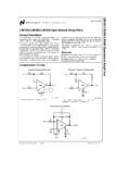
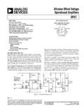
3 2% to 98% High Level Outputs .. TTL to 28V Simultaneous Sine, Square, and Triangle WaveOutputs Easy to Use - Just a Handful of External ComponentsRequiredPinoutICL8038(PDIP, CERDIP)TOP VIEWF unctional DiagramOrdering InformationPART NUMBERSTABILITYTEMP. RANGE (oC)PACKAGEPKG. (Typ)0 to 7014 Ld (Typ)0 to 7014 Ld (Typ)0 to 7014 Ld (Typ)0 to 7014 Ld CYCLEV+FM BIASNCNCSINE WAVEV- OR GNDTIMINGSQUAREFM SWEEP1234567141312111098 ADJUSTCAPACITORWAVE OUTINPUTSINE WAVEADJUSTWAVE OUTOUTFREQUENCYADJUSTCOMPARATOR#1 COMPARATOR#2 FLIP-FLOPSINECONVERTERBUFFERBUFFER9211I1 06V+V- OR GNDCURRENTSOURCE#1 CURRENTSOURCE#22IC3 September 1998 File Number Maximum RatingsThermal InformationSupply Voltage (V- to V+).
4 36 VInput Voltage (Any Pin) .. V- to V+Input Current (Pins 4 and 5).. 25mAOutput Sink Current (Pins 3 and 9) .. 25mAOperating ConditionsTemperature RangeICL8038AC, ICL8038BC, ICL8038CC .. 0oC to 70oCThermal Resistance (Typical, Note 1) JA (oC/W) JC (oC/W)CERDIP Package ..7520 PDIP Package ..115N/AMaximum Junction Temperature (Ceramic Package) ..175oCMaximum Junction Temperature (Plastic Package) ..150oCMaximum Storage Temperature Range .. -65oC to 150oCMaximum Lead Temperature (Soldering 10s).
5 300oCDie CharacteristicsBack Side Potential .. V-CAUTION: Stresses above those listed in Absolute Maximum Ratings may cause permanent damage to the device. This is a stress only rating and operationofthedevice at these or any other conditions above those indicated in the operational sections of this specification is not :1. JA is measured with the component mounted on an evaluation PC board in free SpecificationsVSUPPLY = 10V or +20V, TA = 25oC, RL = 10k , Test Circuit Unless Otherwise SpecifiedPARAMETERSYMBOLTESTCONDITIONSIC L8038 CCICL8038 BCICL8038 ACUNITSMINTYPMAXMINTYPMAXMINTYPMAXS upply Voltage Operating RangeVSUPPLYV+Single Supply+10-+30+10-+30+10-+30VV+, V-Dual Supplies 5- 15 5- 15 5- 15 VSupply CurrentISUPPLYVSUPPLY = 10V(Note 2)1220-1220-1220mAFREQUENCY CHARACTERISTICS (All Waveforms)Max.
6 Frequency of OscillationfMAX100--100--100--kHzSweep Frequency of FM InputfSWEEP-10- -10- -10-kHzSweep FM Range(Note 3)-35:1--35:1--35:1-FM Linearity10:1 Drift withTemperature (Note 5) f/ T0oC to 70oC-250--180--120ppm/oCFrequency Drift with Supply Voltage f/ VOver SupplyVoltage CHARACTERISTICSS quare WaveLeakage CurrentIOLKV9 = 30V--1--1--1 ASaturation VoltageVSATISINK = TimetRRL = -180--180--180-nsFall TimetFRL = -40- -40- -40-nsTypical Duty Cycle Adjust(Note 6) D2982-982-98%Triangle/Sawtooth/Ramp-Ampl itudeVTRIAN-GLERTRI = 100k ImpedanceZOUTIOUT = 5mA-200--200--200- ICL80383 Sine WaveAmplitudeVSINERSINE = 100k = 1M (Note 4) AdjustedTHDUse Figure :2.
7 RA and RB currents not VSUPPLY = 20V; RA and RB = 10k , f 10kHz nominal; can be extended 1000 to 1. See Figures 5A and 82k connected between pins 11 and 12, Triangle Duty Cycle set at 50%. (Use RA and RB.)5. Figure 1, pins 7 and 8 connected, VSUPPLY = 10V. See Typical Curves for vs Not tested, typical value for design purposes SpecificationsVSUPPLY = 10V or +20V, TA = 25oC, RL = 10k , Test Circuit Unless Otherwise Specified (Continued)PARAMETERSYMBOLTESTCONDITIONS ICL8038 CCICL8038 BCICL8038 ACUNITSMINTYPMAXMINTYPMAXMINTYPMAXTest ConditionsPARAMETERRARBRLCSW1 MEASURES upply Current10k 10k 10k Into Pin 6 Sweep FM Range (Note 7)
8 10k 10k 10k at Pin 9 Frequency Drift with Temperature10k 10k 10k at Pin 3 Frequency Drift with Supply Voltage (Note 8)10k 10k 10k at Pin 9 Output Amplitude (Note 10)Sine10k 10k 10k Output at Pin 2 Triangle10k 10k 10k Output at Pin 3 Leakage Current (Off) (Note 9)10k 10k into Pin 9 Saturation Voltage (On) (Note 9)10k 10k (Low) at Pin 9 Rise and Fall Times (Note 11)10k 10k at Pin 9 Duty Cycle Adjust (Note 11)Max50k ~ 10k at Pin 9 Min~25k 50k 10k at Pin 9 Triangle Waveform Linearity10k 10k 10k at Pin 3 Total Harmonic Distortion10k 10k 10k at Pin 2 NOTES:7.
9 The hi and lo frequencies can be obtained by connecting pin 8 to pin 7 (fHI) and then connecting pin 8 to pin 6 (fLO). Otherwise apply SweepVoltage at pin 8 (2/3 VSUPPLY+2V) VSWEEP VSUPPLY where VSUPPLYis the total supply voltage. In Figure 5B, pin 8 should vary and 10V with respect to 10V V+ 30V, or 5V VSUPPLY Oscillation can be halted by forcing pin 10 to +5V or Output Amplitude is tested under static conditions by forcing pin 10 to 5V then to Not tested; for design purposes CircuitApplication Information(See Functional Diagram)An external capacitor C is charged and discharged by twocurrent sources.
10 Current source #2 is switched on and off by aflip-flop, while current source #1 is on continuously. Assumingthat the flip-flop is in a state such that current source #2 is off,and the capacitor is charged with a current I, the voltageacross the capacitor rises linearly with time. When this voltagereaches the level of comparator #1 (set at 2/3 of the supplyvoltage), the flip-flop is triggered, changes states, andreleases current source #2. This current source normallycarries a current 2I, thus the capacitor is discharged with anet-current I and the voltage across it drops linearly with it has reached the level of comparator #2 (set at 1/3 ofthe supply voltage), the flip-flop is triggered into its originalstate and the cycle starts waveforms are readily obtainable from this basicgenerator circuit.