Transcription of ICL8038
1 1 SemiconductorCAUTION: These devices are sensitive to electrostatic discharge; follow proper IC Handling Harris Corporation 1998 ICL8038 Precision Waveform Generator/VoltageControlled OscillatorThe ICL8038 waveform generator is a monolithic integratedcircuit capable of producing high accuracy sine, square,triangular, sawtooth and pulse waveforms with a minimum ofexternal components. The frequency (or repetition rate) canbe selected externally from to more than 300kHzusing either resistors or capacitors, and frequencymodulation and sweeping can be accomplished with anexternal voltage. The ICL8038 is fabricated with advancedmonolithic technology, using Schottky barrier diodes and thinfilm resistors, and the output is stable over a wide range oftemperature and supply variations.
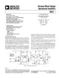
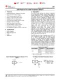
2 These devices may beinterfaced with phase locked loop circuitry to reducetemperature drift to less than 250 Low Frequency Drift with Temperature ..250ppm/oC Low Distortion.. 1% (Sine Wave Output) High Linearity .. (Triangle Wave Output) Wide Frequency Range .. to 300kHz Variable Duty Cycle .. 2% to 98% High Level Outputs .. TTL to 28V Simultaneous Sine, Square, and Triangle WaveOutputs Easy to Use - Just a Handful of External ComponentsRequiredPinoutICL8038(PDIP, CERDIP)TOP VIEWF unctional DiagramOrdering InformationPART NUMBERSTABILITYTEMP. RANGE (oC)PACKAGEPKG. (Typ)0 to 7014 Ld (Typ)0 to 7014 Ld (Typ)0 to 7014 Ld (Typ)0 to 7014 Ld CYCLEV+FM BIASNCNCSINE WAVEV- OR GNDTIMINGSQUAREFM SWEEP1234567141312111098 ADJUSTCAPACITORWAVE OUTINPUTSINE WAVEADJUSTWAVE OUTOUTFREQUENCYADJUSTCOMPARATOR#1 COMPARATOR#2 FLIP-FLOPSINECONVERTERBUFFERBUFFER9211I1 06V+V- OR GNDCURRENTSOURCE#1 CURRENTSOURCE#22IC3 September 1998 File Number Maximum RatingsThermal InformationSupply Voltage (V- to V+).
3 36 VInput Voltage (Any Pin) .. V- to V+Input Current (Pins 4 and 5).. 25mAOutput Sink Current (Pins 3 and 9) .. 25mAOperating ConditionsTemperature RangeICL8038AC, ICL8038BC, ICL8038CC .. 0oC to 70oCThermal Resistance (Typical, Note 1) JA (oC/W) JC (oC/W)CERDIP Package ..7520 PDIP Package ..115N/AMaximum Junction Temperature (Ceramic Package) ..175oCMaximum Junction Temperature (Plastic Package) ..150oCMaximum Storage Temperature Range .. -65oC to 150oCMaximum Lead Temperature (Soldering 10s) .. 300oCDie CharacteristicsBack Side Potential .. V-CAUTION: Stresses above those listed in Absolute Maximum Ratings may cause permanent damage to the device. This is a stress only rating and operationofthedevice at these or any other conditions above those indicated in the operational sections of this specification is not :1.
4 JA is measured with the component mounted on an evaluation PC board in free SpecificationsVSUPPLY = 10V or +20V, TA = 25oC, RL = 10k , Test Circuit Unless Otherwise SpecifiedPARAMETERSYMBOLTESTCONDITIONSIC L8038 CCICL8038 BCICL8038 ACUNITSMINTYPMAXMINTYPMAXMINTYPMAXS upply Voltage Operating RangeVSUPPLYV+Single Supply+10-+30+10-+30+10-+30VV+, V-Dual Supplies 5- 15 5- 15 5- 15 VSupply CurrentISUPPLYVSUPPLY = 10V(Note 2)1220-1220-1220mAFREQUENCY CHARACTERISTICS (All Waveforms)Max. Frequency of OscillationfMAX100--100--100--kHzSweep Frequency of FM InputfSWEEP-10- -10- -10-kHzSweep FM Range(Note 3)-35:1--35:1--35:1-FM Linearity10:1 Drift withTemperature (Note 5) f/ T0oC to 70oC-250--180--120ppm/oCFrequency Drift with Supply Voltage f/ VOver SupplyVoltage CHARACTERISTICSS quare WaveLeakage CurrentIOLKV9 = 30V--1--1--1 ASaturation VoltageVSATISINK = TimetRRL = -180--180--180-nsFall TimetFRL = -40- -40- -40-nsTypical Duty Cycle Adjust(Note 6) D2982-982-98%Triangle/Sawtooth/Ramp-Ampl itudeVTRIAN-GLERTRI = 100k ImpedanceZOUTIOUT = 5mA-200--200--200- ICL80383 Sine WaveAmplitudeVSINERSINE = 100k = 1M (Note 4) AdjustedTHDUse Figure :2.
5 RA and RB currents not VSUPPLY = 20V; RA and RB = 10k , f 10kHz nominal; can be extended 1000 to 1. See Figures 5A and 82k connected between pins 11 and 12, Triangle Duty Cycle set at 50%. (Use RA and RB.)5. Figure 1, pins 7 and 8 connected, VSUPPLY = 10V. See Typical Curves for vs Not tested, typical value for design purposes SpecificationsVSUPPLY = 10V or +20V, TA = 25oC, RL = 10k , Test Circuit Unless Otherwise Specified (Continued)PARAMETERSYMBOLTESTCONDITIONS ICL8038 CCICL8038 BCICL8038 ACUNITSMINTYPMAXMINTYPMAXMINTYPMAXTest ConditionsPARAMETERRARBRLCSW1 MEASURES upply Current10k 10k 10k Into Pin 6 Sweep FM Range (Note 7)10k 10k 10k at Pin 9 Frequency Drift with Temperature10k 10k 10k at Pin 3 Frequency Drift with Supply Voltage (Note 8)10k 10k 10k at Pin 9 Output Amplitude (Note 10)Sine10k 10k 10k Output at Pin 2 Triangle10k 10k 10k Output at Pin 3 Leakage Current (Off) (Note 9)10k 10k into Pin 9 Saturation Voltage (On) (Note 9)10k 10k (Low) at Pin 9 Rise and Fall Times (Note 11)
6 10k 10k at Pin 9 Duty Cycle Adjust (Note 11)Max50k ~ 10k at Pin 9 Min~25k 50k 10k at Pin 9 Triangle Waveform Linearity10k 10k 10k at Pin 3 Total Harmonic Distortion10k 10k 10k at Pin 2 NOTES:7. The hi and lo frequencies can be obtained by connecting pin 8 to pin 7 (fHI) and then connecting pin 8 to pin 6 (fLO). Otherwise apply SweepVoltage at pin 8 (2/3 VSUPPLY+2V) VSWEEP VSUPPLY where VSUPPLYis the total supply voltage. In Figure 5B, pin 8 should vary and 10V with respect to 10V V+ 30V, or 5V VSUPPLY Oscillation can be halted by forcing pin 10 to +5V or Output Amplitude is tested under static conditions by forcing pin 10 to 5V then to Not tested; for design purposes CircuitApplication Information(See Functional Diagram)An external capacitor C is charged and discharged by twocurrent sources.
7 Current source #2 is switched on and off by aflip-flop, while current source #1 is on continuously. Assumingthat the flip-flop is in a state such that current source #2 is off,and the capacitor is charged with a current I, the voltageacross the capacitor rises linearly with time. When this voltagereaches the level of comparator #1 (set at 2/3 of the supplyvoltage), the flip-flop is triggered, changes states, andreleases current source #2. This current source normallycarries a current 2I, thus the capacitor is discharged with anet-current I and the voltage across it drops linearly with it has reached the level of comparator #2 (set at 1/3 ofthe supply voltage), the flip-flop is triggered into its originalstate and the cycle starts waveforms are readily obtainable from this basicgenerator circuit.
8 With the current sources set at I and 2 Irespectively, the charge and discharge times are equal. Thusa triangle waveform is created across the capacitor and theflip-flop produces a square wave. Both waveforms are fed tobuffer stages and are available at pins 3 and +10 VFIGURE 1. TEST CIRCUITQ20Q21Q19Q22Q31Q32Q33Q34Q30Q7Q6Q1 Q2Q4Q8Q9Q5Q3Q14Q11Q12Q13Q24Q23Q25Q26Q29Q 27Q28Q10Q15Q18Q17Q16Q35Q36Q38Q40Q37Q39R1 11KR239K7854 REXT BREXT ACOMPARATORR414KR85KR95KR105KR4327KR4227 KBUFFER CONVERTERQ49Q50Q52Q51Q53Q55Q54Q56Q42Q41Q 43Q44Q45Q46Q47Q486V+ SOURCES911 ICL80385 The levels of the current sources can, however, be selectedover a wide range with two external resistors. Therefore, withthe two currents set at values different from I and 2I, anasymmetrical sawtooth appears at Terminal 3 and pulseswith a duty cycle from less than 1% to greater than 99% areavailable at Terminal sine wave is created by feeding the triangle wave into anonlinear network (sine converter).
9 This network provides adecreasing shunt impedance as the potential of the trianglemoves toward the two TimingThesymmetry of all waveforms can be adjusted with theexternal timing resistors. Two possible ways to accomplishthis are shown in Figure 3. Best results are obtained bykeeping the timing resistors RA and RB separate (A). RAcontrols the rising portion of the triangle and sine wave andthe 1 state of the square magnitude of the triangle waveform is set at1/3 VSUPPLY; therefore the rising portion of the triangle is,The falling portion of the triangle and sine wave and the 0state of the square wave is:Thus a 50% duty cycle is achieved when RA = the duty cycle is to be varied over a small range about 50%only, the connection shown in Figure 3B is slightly moreconvenient.
10 A 1k potentiometer may not allow the duty cycleto be adjusted through 50% on all devices. If a 50% duty cycleis required, a 2k or 5k potentiometer should be two separate timing resistors, the frequency is given by:or, if RA = RB = Rt1CV I--------------C 1/3 VSUPPLYRA VSUPPLY ---------------------------------------- ---------------------------RAC 1-------------C1 /3 VSUPPLY 2 () 2 RARB ()-------------------------------------- ===f1t1t2+ -------------------------+ ---------------------------------------- --------------== (for Figure 3A)=FIGURE 2A. SQUARE WAVE DUTY CYCLE - 50%FIGURE 2B. SQUARE WAVE DUTY CYCLE - 80%FIGURE 2. PHASE RELATIONSHIP OF WAVEFORMSFIGURE 3. POSSIBLE CONNECTIONS FOR THE EXTERNAL TIMING RESISTORSC82 KICL80384569212111087 RARLV- OR GND3 RBV+ICL80384569212111087C100 KRARLV- OR GND3 RBV+1k ICL80386 Neither time nor frequency are dependent on supply voltage,even though none of the voltages are regulated inside theintegrated circuit.