Example: quiz answers
INFORMATION TECHNOLOGY - 802 CLASS XI SESSION 2020 …
INFORMATION TECHNOLOGY - 802 ... RAM is of two types : DRAM (Dynamic Random Access Memory) and SRAM ( Static Random Access Memory. DRAM SRAM Used in main memory It is used in cache Inexpensive Expensive . Uses less power Uses more power Slower than SRAM Faster than DRAM 2. ROM ( Read Only Memory) : It is generally used in startup …
Tags:
Information
Domain:
Source:
Link to this page:
Documents from same domain
Sample Question Paper (PHYSICS) CLASS-XII (2017 …
cbseacademic.nic.in1 Sample Question Paper (PHYSICS) CLASS-XII (2017-18) Time Allowed: 3Hours Maximum Marks: 70 General Instructions 1. All questions are compulsory.

CBSE SAMPLE PAPER -2016-17
cbseacademic.nic.incbse sample paper -2016-17 * value based question a(b) where; a = number of questions; b= marks hence 26 (70) name of the unit total weigh tage

SENIOR SCHOOL CURRICULUM 2018-19 VOLUME III (i) …
cbseacademic.nic.inclass SENIOR SCHOOL CURRICULUM 2018-19 VOLUME III (i) Carnatic Music Effective from the academic session 2018-19 for - XI and XII

KWHS Global Investment Management Competition KWHS …
cbseacademic.nic.in“शिक्षा सदन”] 17, राउज एवेन्यु, नई ददल्ली-110 002 “Shiksha Sadan”, 17, Rouse Avenue, New Delhi – 110 ...
CHEMISTRY (Code No. 043) 2019-20
cbseacademic.nic.inCHEMISTRY (Code No. 043) 2019-20 Rationale Higher Secondary is the most crucial stage of school education because at this juncture specialized discipline based, content -oriented courses are introduced.
Entrepreneurial Skills Introduction
cbseacademic.nic.ininvolved in combining ingredients to make different products, they are performing a ... inventory – Raw material, Work-in-progress and Finished goods ... already employed, they were still curious to know the options available out there. This

SOCIAL SCIENCE - CBSE
cbseacademic.nic.inSOCIAL SCIENCE CLASS IX-X (2020-21) (CODE NO. 087) Rationale Social Science is a compulsory subject up to secondary stage of school education. It is an integral component of general education because it helps the learners to understand the environment in its totality and developing a broader perspective and an empirical,

SOCIAL SCIENCE - CBSE
cbseacademic.nic.inSOCIAL SCIENCE CLASS IX-X (2021-22) (CODE NO. 087) Rationale Social Science is a compulsory subject up to secondary stage of school education. It is an integral component of general education because it helps the learners to understand the environment in its totality and developing a broader perspective and an empirical,
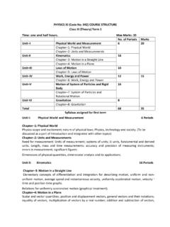
PHYSICS XI (Code No. 042) COURSE STRUCTURE Class XI ...
cbseacademic.nic.inPHYSICS XI (Code No. 042) COURSE STRUCTURE Class XI (Theory) Term 1 Time: one and half hours. Max Marks: 35 No. of Periods Marks Unit–I Physical World and Measurement 6 20 Chapter–1: Physical World Chapter–2: Units and Measurements Unit-II Kinematics 16 Chapter–3: Motion in a Straight Line Chapter–4: Motion in a Plane

ART EDUCATION (CODE No. 502) - cbseacademic.nic.in
cbseacademic.nic.inART EDUCATION (CODE No. 502) Rationale Art education constitutes an important area of curricular activity for the development of the wholesome personality of the learners. Art is a process of fulfilment running through every aspect of life and it goes on in a creative, productive and joyful manner.
Related documents

TN-46-05 GENERAL DDR SDRAM ... - Micron Technology
www.micron.comGeneral DDR SDRAM Functionality 3 Micron Technology, Inc., reserves the right to change products or specifications without notice. TN4605.p65 – Rev. A; Pub. 7/01 ©2001, Micron Technology, Inc. TN-46-05 GENERAL DDR SDRAM FUNCTIONALITY n-bit Data Register n-bit Data Register CLKD n-bit data plus DQS Q D0 MUX D1 C DQS From DRAM Core 2n-bit data ...

NAND vs. NOR Flash Memory Technology Overview
aturing.umcs.maine.eduApr 25, 2006 · Flash memory, Pseudo SRAM and/or low power DRAM in a single package by using chip-stacking technology. This advanced packaging technology enables a complete memory subsystem with different types of semiconductor memory to be packaged as a single component to reduce size and contribute to cost reduction for cellular phones and other …

LPDDR3 and LPDDR4 - JEDEC
www.jedec.orgReducing Power in DRAM •DRAM core power usage –Generally a function of device organization, usage, manufacturing technology •Standby power –Available features for controlling power •IO signaling power –Function of voltage swing, termination, IO capacitance, frequency, load, …
TN-40-07: Calculating Memory Power for DDR4 SDRAM
www.micron.comAs noted, DDR4 technology added a VPP supply for the DRAM internal word line boost. A key difference between the DDR4 Power Calculator and the DDR3 Power Calculator is the DDR4 Power Calculator (both available on micron.com) includes VPP power cover-age.
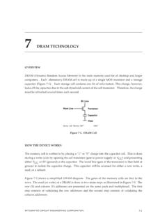
DRAM Technology - Smithsonian Institution
smithsonianchips.si.eduDRAM Technology INTEGRATED CIRCUITENGINEERING CORPORATION 7-7 256K 1M 4M 16M 64M 256M 1G 4G 10-1 1 101 102 103 10 1.0 0.1 0.01 DRAM Generation (bits) Chip Area (mm 2), Cell Area (µ m 2) Minim um Feature Siz e (µ m 2) Source: Hitachi/ICE, "Memory 1997" 20775A Cell Area Chip Area Minimum Feature Size Figure 7-10. DRAM Technology Trend

Introduction to Integrated Circuit Technology
www.icknowledge.cominteract with have a strong understanding of IC technology, but there is also a substantial group that purchases or uses the technology without a strong understanding. For the later group, we though it would be useful to produce a basic introduction to IC technology, and that is the objec-tive of this publication.

Technology and Cost Trends at Advanced Nodes
www.icknowledge.com• DRAM scaling has slowed with a possible long term 3D STT MRAM transition. • 3D NAND is positioned to scale into the 2020s with terabit memories on the horizon. • 3D XPoint is a complementary technology to DRAM and 3D NAND for storage class memory applications. • 3D everything is the future of leading edge.

DRAM Design Overview - Stanford University
www.graphics.stanford.eduDRAM Design Overview Junji Ogawa 90 92 94 96 98 00 02 04 06 08 10 1000 100 20 50 200 500 64M 256M 1G Die Size(mm2) Early Production 256M Production 1G 4G 0.35 0.18 0.13 0.10 Rule (um) Year i-line ArF ? 16M 0.50 64M 0.25 4G KrF 128M KrF+α Standard DRAM Development Conference Feb. 11th. 1998 DRAM Design Overview Junji Ogawa Bit Cost Trend of ...