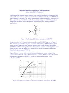
Transcription of IXYS POWER MOSFETs Datasheet Definition
1 ixys PowerMOSFET Datasheet Parameters DefinitionAbdus Sattar, ixys CorporationIXAN00651 ixys providesdatasheets with parametersthat areessential andusefulforselectingthe appropriate device as well asfor predetectingits performance in anapplication. Thegraphs included in the Datasheet representtypical performancecharacteristicandcan be used to extrapolate from one set of operating conditions toanother. POWER MOSFET generally contains a bodydiode, whichprovides freewheeling operation intheinductive load 1 shows the equivalentcircuitforanN-Channelanda P-Channel POWER 1: (a)anN-Channel (b)a P-Channel Enhancement-Mode POWER MOSFET1 EssentialRatings andCharacteristics1.
2 MaximumRatingsThe ratings are limiting values for a deviceand validfor the whole range of TJandTJMThe junction temperature(JT) range is-55 ~ 150oC in most cases andit is thedevice s permissible temperaturerangewithin which the device may beoperatedcontinuously. The maximum junction temperature (JMT) is 150oC unlessotherwise specified(in some cases 175oC). Junction temperature varies electricalparametersof POWER MOSFET, for example, atvery low temperature (<-55oC),the device can loss itsfunctionalityand atvery high temperature,the device sthreshold voltage becomes very lowandleakage current becomes very high.
3 Italso cancause thermal run awaywithin the deviceat very high TemperatureTStgIt is the range of temperaturefor storage or transportation of the dev ice and itmust be between-55 ~ Temperature TLIt is the maximum leadtemperatureduring soldering and it must not exceed300oC for 10 seconds at 1/8 from the PDIXYS PowerMOSFET Datasheet Parameters DefinitionAbdus Sattar, ixys CorporationIXAN00652 The POWER dissipation is the maximumcalculatedpower that the device candissipate and is function of both on the maximum junction temperature and thethermal resistance at a case [TJ M TC]/RthJC(1) Drain Current ID25 This is the maximum current rating for the deviceat a case temperature(TC)25oC.
4 It is calculated based on maximum POWER dissipation, maximum on-resistance and temperature dependence of on-resistance. It canbe limited by thecurrent handling capacity of IDRMSThis is the maximum current ratingofthe device s lead at a case Current IDMIt is the peak current the device can flow above ID25specification under themaximum junction temperature. It varies with current pulse widths, duty cycleand heat dissipation Forward Current ISIt s the maximum DC current the diode can flow in the forward direction atspecified case Diode ForwardCurrent ISMIt s thepeakcurrent the diode can flowabove ISspecification under the maximumjunction Drain-Source Voltage VDSSThis is defined as the maximumdrain-source voltage without causing avalanchebreakdown with gate-source short-circuited (VGS= 0)
5 And the device is at avalanche breakdown voltage is temperature dependent and could be lessthan theBVDSS, VGSThis is the maximumvoltage that can be introduced between gate and source. Itdepends on the thickness and characteristics of the gate oxide layer. The actualgate oxide withstand voltage is typically much higher than this but varies due tomanufacturing processes, so staying within this rating ensures ofRise ofOff -stateVoltage (dv/dt)This isdefined as the maximum permissible rate of rise of off-state voltage acrossthe Energy(for avalanche devices) ,RepetitiveIARIXYS PowerMOSFET Datasheet Parameters DefinitionAbdus Sattar, ixys CorporationIXAN00653 For POWER MOSFETs , the propensity for current crowding in the die area duringavalanche mandates a limit in avalanche current.
6 It represents the avalancheenergy specification for thedevice andthetrue capability of a repetitiveAvalanche Energy, Single Pulse EARThe maximum permissible reverse-voltagebreakdown energy in continuousoperationwhile observing the maximum permissiblechip heatdissipation limits the avalanche non-repetitiveAvalanche Energy, EASThe maximum permissible reverse-voltagebreakdown energy in continuousoperationwhile observing the maximum permissiblechip heatdissipation limitsthe avalanche Mechanical provides the mechanical size of the device with package provides the weight information of the devicewith TorqueMdThis provides the maximum permissibletorque that can be applied on the devicefor CharacteristicsAccording to IEC 60747-8.
7 2004, the characteristics of POWER MOSFETs are given at25 Coand at one specified higher operating IGSSIt is the maximum gate-source leakage current with the drain and thesourceshortedandwiththe introduction of rated gate-source IDSSIt is the maximum drain-source leakage current with the gate and the sourceshortedandwith the introduction of rated drain-source Down Voltage BVDSST hebreakdown voltageBVDSSis the minimum blocking voltage between thedrain and the source at given drain currentand when the gate is shorted to break down voltage has a positive temperature Threshold VoltageVGS (th)It is the gate-source voltage at which the drain current starts to flowand thedevice is considered at ON-State.
8 It has negative temperature PowerMOSFET Datasheet Parameters DefinitionAbdus Sattar, ixys on-state voltageVGSMThis is agate-source maximum voltage in the On-state ResistanceRDS (on)The specific on-resistance for a POWER MOSFET is defined byRDS (on)= RSOURCE+ RCH+ RA+ RD+ RJ+ Rsub+ Rwcml,(2)Where,RSOURCE= Source diffusion resistanceRCH= Channel resistanceRA= Accumulation resistanceRJ= JFET component resistanceRD= Drift region resistanceRsub= Substrate resistanceRwcml= Bond wire TransconductancegfsIt is defined as the change in drain current divided by the change in gate voltagefor a constant drain large transconductance is desirable to obtain a highcurrent handling capabilitywith low gate drive voltage and for achieving highfrequency Capacitances andGate Capacitance CissThe input capacitance is measured between the gate and source terminals with thedrain shorted to the source terminal.
9 The Cissis made up of the gate-to -draincapacitance CDGin parallel with the gate-to -source capacitance CGS+CDG(3) Transfer Capacitance CrssThe reverse transfer capacitance is measured between the drain and gate terminalswith the source connected to ground. The reverse transfer capacitance is the sameas the gate-to -drain capacitance CDG(4) Capacitance CossThe output capacitance is measured between the drain and source with the gateshorted to the source terminal. The Cossis equal to the drain-to -source capacitanceCDS, in parallel with the gate to drain capacitance CDS+CDG(5) ChargesIt s the total gate charge that s required to raise the gate-source voltage to 15 Vinmost casesto fully turn-on the device.
10 It smeasured at a specified drain current, ixys PowerMOSFET Datasheet Parameters DefinitionAbdus Sattar, ixys CorporationIXAN00655drain-source voltage and gate-source gatechargereflects the chargestored on the inter-terminal capacitances described earlier and is used in designingth e gate drive Switching times(td (on),tr,td (off),tf) Delay Time td (on)The turn-on delay time is defined as the time interval when the gate-sourcevoltage(VGS) has reached 10 % of its end value (VGG), to the time when the drain-source voltage(VDS) hasdropped to 90 % of its initial value (VDD). Time trFollowing the turn-on delay time, the rise-time follows; it is the interval betweenthe drain-source voltages from 90% to 10% of its initial value.