Transcription of LECTURE 390 – OPEN-LOOP COMPARATORS
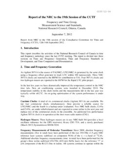
1 LECTURE 390 OPEN-LOOP COMPARATORS (4/8/02) Page 390-1. LECTURE 390 OPEN-LOOP COMPARATORS . (READING: AH 461-475). Objective The objective of this presentation is: 1.) Show other types of continuous- time , OPEN-LOOP COMPARATORS 2.) Improve the performance of continuous- time , OPEN-LOOP COMPARATORS Outline Push-pull COMPARATORS COMPARATORS that can drive large capacitors Autozeroing techniques COMPARATORS using hysteresis Summary ECE 6412 - Analog Integrated Circuit Design - II Allen - 2002. LECTURE 390 OPEN-LOOP COMPARATORS (4/8/02) Page 390-2. Push-Pull COMPARATORS Clamped: VDD. M4 M6. M3 M8. vout - M1 M2. vin CL. +. M5. + M9 M7. VBias - VSS Fig. Comments: Gain reduced Larger input resolution Push-pull output Higher slew rates ECE 6412 - Analog Integrated Circuit Design - II Allen - 2002.
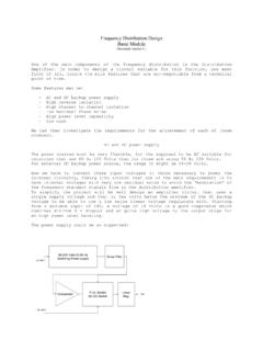
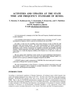
2 LECTURE 390 OPEN-LOOP COMPARATORS (4/8/02) Page 390-3. Push-Pull COMPARATORS - Improved Cascode output stage: VDD. M4 M6. M15. M3 M8. M14 M7. R1 R2 vout - M1 M2 M9. vin M12 CII. + M10. M5 M11. + M13. VBias - VSS Fig. Comments: Can also use the folded cascode architecture Cascode output stage result in a slow linear response (dominant pole is small). Poorer noise performance ECE 6412 - Analog Integrated Circuit Design - II Allen - 2002. LECTURE 390 OPEN-LOOP COMPARATORS (4/8/02) Page 390-4. COMPARATORS that Can Drive Large Capacitive Loads VDD. M8 M10. M3 M4. M6. - M1 M2 vout vin + CII. + M7 M9 M11. VBias M5. - VSS Fig. Comments: Slew rate = 3V/ s into 50pF. Linear rise/fall time = 100ns into 50pF.
3 Propagation delay time 1 s Loop gain 32,000 V/V. ECE 6412 - Analog Integrated Circuit Design - II Allen - 2002. LECTURE 390 OPEN-LOOP COMPARATORS (4/8/02) Page 390-5. Self-Biased Differential Amplifier . VDD. VDD. VBias M6 Extremely M6 large sourcing M3 M4 current M3 M4. vout vin+ vin- vin+ vin- M1 M2. M1 M2. M5. VBias M5. VSS Fig. VSS. Advantage: Large sink or source current with out a large quiescent current. Disadvantage: Poor common mode range (vin+ slower than vin-).. M. Bazes, Two Novel Full Complementary Self-Biased CMOS Differential Amplifiers, IEEE Journal of Solid-State Circuits, Vol. 26, No. 2, Feb. 1991, pp. 165-168. ECE 6412 - Analog Integrated Circuit Design - II Allen - 2002.
4 LECTURE 390 OPEN-LOOP COMPARATORS (4/8/02) Page 390-6. Autozeroing Techniques Use the comparator as an op amp to sample the dc input offset voltage and cancel the offset during operation. Ideal Ideal Ideal Comparator Comparator Comparator vIN. - - - vOUT. + + - +. VOS VOS CAZ VOS + VOS. + VOS. -C. AZ. Model of Comparator. Autozero Cycle Comparison Cycle Fig. Comments: The comparator must be stable in the unity-gain mode (self-compensating COMPARATORS are good, the two-stage op comparator would require compensation to be switched in during the autozero cycle.). Complete offset cancellation is limited by charge injection ECE 6412 - Analog Integrated Circuit Design - II Allen - 2002. LECTURE 390 OPEN-LOOP COMPARATORS (4/8/02) Page 390-7.
5 Differential Implementation of Autozeroed COMPARATORS 1 Ideal vIN- + - vOUT = VOS. Comparator VOS. 2 - +. - vOUT. 1 VOS. vIN+ + Comparator during 1 phase 2 VOS vIN - - vOUT. CAZ 1 +. vIN+ + - VOS VOS. Differential Autozeroed Comparator Comparator during 2 phase Fig. ECE 6412 - Analog Integrated Circuit Design - II Allen - 2002. LECTURE 390 OPEN-LOOP COMPARATORS (4/8/02) Page 390-8. Single-Ended Autozeroed COMPARATORS Noninverting: 2 - 1. 1 CAZ vOUT. vIN +. 2. 1. Fig. Inverting: CAZ. vIN vOUT. 2 - 1. 1 +. Fig. Comment on autozeroing: Need to be careful about noise that gets sampled onto the autozeroing capacitor and is present on the comparison phase of the process. ECE 6412 - Analog Integrated Circuit Design - II Allen - 2002.
6 LECTURE 390 OPEN-LOOP COMPARATORS (4/8/02) Page 390-9. Influence of Input Noise on the Comparator Comparator without hysteresis: Comparator vin threshold t vout VOH. t VOL Fig. Comparator with hysteresis: vin VTRP+. t VTRP- vout VOH. t VOL. Fig. ECE 6412 - Analog Integrated Circuit Design - II Allen - 2002. LECTURE 390 OPEN-LOOP COMPARATORS (4/8/02) Page 390-10. Use of Hysteresis for COMPARATORS in a Noisy Environment Transfer curve of a comparator with hysteresis: vOUT vOUT. VOH VOH. VTRP+ R1 (V -V ). R2 OH OL VTRP+. vIN 0 vIN. 0. VTRP- VTRP- VOL VOL. Counterclockwise Bistable Clockwise Bistable Fig. Hysteresis is achieved by the use of positive feedback Externally Internally ECE 6412 - Analog Integrated Circuit Design - II Allen - 2002.
7 LECTURE 390 OPEN-LOOP COMPARATORS (4/8/02) Page 390-11. Noninverting Comparator using External Positive Feedback Circuit: vOUT. V OH. R2. R1 (V -V ) R1 VOH. vIN R1 R2 OH OL. + vOUT 0 R2. vIN. - R1 VOL 0. R2. VOL. Fig. Upper Trip Point: Assume that vOUT = VOL, the upper trip point occurs when, R1 R2 R1. 0 = R1+R2 VOL + R1+R2 VTRP+.. VTRP+ = - R2 VOL.. Lower Trip Point: Assume that vOUT = VOH, the lower trip point occurs when, R1 R2 R1. 0 = R +R VOH + R +R VTRP- V TRP. -=- R2 VOH. 1 2 1 2 . Width of the bistable characteristic: R1 .. Vin = VTRP+-VTRP- = R VOH -VOL . 2 . ECE 6412 - Analog Integrated Circuit Design - II Allen - 2002. LECTURE 390 OPEN-LOOP COMPARATORS (4/8/02) Page 390-12.
8 Inverting Comparator using External Positive Feedback Circuit: vOUT. VOH. vIN - vOUT R1 (V -V ). + R1+R2 OH OL. 0 vIN. 0. R2 R1 VOL R1 VOH. R1 R1+R2. R1+R2 VOL. Fig. Upper Trip Point: R . 1 . vIN = VTRP = R +R VOH. + . 1 2 . Lower Trip Point: R . 1 . vIN = VTRP = R +R VOL. - . 1 2 . Width of the bistable characteristic: R1 .. Vin = VTRP -VTRP = R +R VOH -VOL . + - 1 2 . ECE 6412 - Analog Integrated Circuit Design - II Allen - 2002. LECTURE 390 OPEN-LOOP COMPARATORS (4/8/02) Page 390-13. Horizontal Shifting of the CCW Bistable Characteristic Circuit: vOUT R1 (V -V ). VOH R2 OH OL. R2. R1 R1+R2. vIN. + vOUT R2 VREF. 0 vIN. - 0 R1|VOL|. VREF R1 VOH R2. R2. VOL. Fig. Upper Trip Point: R1 R2 R1+R2 R1.
9 VREF = R +R VOL + R +R VTRP+ VTRP+ = R2 VREF - R2 VOL. 1 2 1 2 . Lower Trip Point: R R R +R R1. 1 2 1 2. VREF = R +R VOH + R +R VTRP- VTRP- = R VREF - R VOH. 1 2 1 2 2 2. Shifting Factor: R1+R2 .. R V. 2 REF.. ECE 6412 - Analog Integrated Circuit Design - II Allen - 2002. LECTURE 390 OPEN-LOOP COMPARATORS (4/8/02) Page 390-14. Horizontal Shifting of the CW Bistable Characteristic Circuit: vOUT R1 (V -V ). vIN - vOUT R1+R2 OH OL. + VOH. R1. R2 R1+R2 VREF. R1 0 vIN. 0 R1 VOH. VREF R1|VOL| R1+R2. R1+R2. VOL. Fig. Upper Trip Point: R 1 R1 . vIN = VTRP + = R +R VOH + R1+R2 V REF.. 1 2 . Lower Trip Point: .. R 1 R. 1 . vIN = VTRP - = R +R VOL + R1+R2 V REF.. 1 2 . Shifting Factor: R1 .. R +R VREF.
10 1 2 . ECE 6412 - Analog Integrated Circuit Design - II Allen - 2002. LECTURE 390 OPEN-LOOP COMPARATORS (4/8/02) Page 390-15. Example Design of an Inverting Comparator with Hysteresis Use the inverting bistable to design a high-gain, OPEN-LOOP comparator having an upper trip point of 1V and a lower trip point of 0V if VOH = 2V and VOL = -2V. Solution Putting the values of this example into the above relationships gives R1 . R1 . 1 = R1+R2 2 + R1+R2 VREF.. and R1 R1 . 0 = R1+R2 (-2) + R1+R2 VREF.. Solving these two equations gives 3R1 = R2 and VREF = 2V. ECE 6412 - Analog Integrated Circuit Design - II Allen - 2002. LECTURE 390 OPEN-LOOP COMPARATORS (4/8/02) Page 390-16. Hysteresis using Internal Positive Feedback Simple comparator with internal positive feedback: VDD.