Transcription of LM3045/LM3046/LM3086 Transistor Arrays - mit.edu
1 TL/H/7950LM3045/LM3046/LM3086 Transistor ArraysDecember 1994LM3045/LM3046/LM3086 Transistor ArraysGeneral DescriptionThe LM3045, LM3046 and LM3086 each consist of fivegeneral purpose silicon NPN transistors on a commonmonolithic substrate. Two of the transistors are internallyconnected to form a differentially-connected pair. The tran-sistors are well suited to a wide variety of applications in lowpower system in the DC through VHF range. They may beused as discrete transistors in conventional circuits howev-er, in addition, they provide the very significant inherent inte-grated circuit advantages of close electrical and thermalmatching.
2 The LM3045 is supplied in a 14-lead cavity dual-in-line package rated for operation over the full military tem-perature range. The LM3046 and LM3086 are electricallyidentical to the LM3045 but are supplied in a 14-lead mold-ed dual-in-line package for applications requiring only a lim-ited temperature matched pairs of transistorsVBEmatchedg5mVInput offset current 2mA max at ICe1mAYFive general purpose monolithic transistorsYOperation from DC to 120 MHzYWide operating current rangeYLow noise dB typ at 1 kHzYFull militarytemperature range (LM3045)
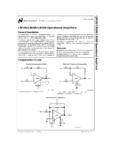
3 B55 Ctoa125 CApplicationsYGeneral use in all types of signal processing systemsoperating anywhere in the frequency range from DC toVHFYC ustom designed differential amplifiersYTemperature compensated amplifiersSchematic and Connection DiagramDual-In-Line and Small Outline PackagesTL/H/7950 1 Top ViewOrder Number LM3045J, LM3046M, LM3046N or LM3086 NSee NS Package Number J14A, M14A or N14AC1995 National Semiconductor CorporationRRD-B30M115/Printed in U. S. Maximum Ratings(TAe25 C)If Military/Aerospace specified devices are required, please contact the National Semiconductor Sales Office/Distributors for availability and Dissipation.
4 TAe25 C300750300750mWTAe25 Cto55 C300750mWTAl55 CDerate at CTAe25 Cto75 C300750mWTAl75 CDerate at 8mW/ CCollector to Emitter Voltage, VCEO1515 VCollector to Base Voltage, VCBO2020 VCollector to Substrate Voltage, VCIO(Note 1)2020 VEmitter to Base Voltage, VEBO55 VCollector Current, IC5050mAOperating Temperature Rangeb55 Ctoa125 Cb40 Ctoa85 CStorage Temperature Rangeb65 Ctoa150 Cb65 Ctoa85 CSoldering InformationDual-In-Line Package Soldering (10 Sec.)260 C260 CSmall Outline PackageVapor Phase (60 Seconds)215 CInfrared (15 Seconds)220 CSee AN-450 Surface Mounting Methods and Their Effect on Product Reliability for other methods of soldering surface Characteristics(TAe25 C unless otherwise specified)LimitsLimitsParameterCondition sLM3045, LM3046LM3086 UnitsMin Typ Max Min Typ MaxCollector to Base Breakdown Voltage (V(BR)CBO)ICe10mA, IEe020602060 VCollector to Emitter Breakdown Voltage (V(BR)CEO)
5 ICe1 mA, IBe015241524 VCollector to Substrate BreakdownICe10mA, ICIe020 6020 60 VVoltage (V(BR)CIO)Emitter to Base Breakdown Voltage (V(BR)EBO)IE10mA, ICe05757 VCollector Cutoff Current (ICBO)VCBe10V, 100 nACollector Cutoff Current (ICEO)VCEe10V, Forward Current TransferVCEe3 VICe10 mA100100 Ratio (Static Beta) (hFE)ICe1 mA 40 10040 100 ICe10mA 5454 Input Offset Current for MatchedVCEe3V, Q1and Q2lIO1bIIO2lBase to Emitter Voltage (VBE) mA of Input Offset Voltage forVCEe3V, PairlVBE1bVBE2lMagnitude of Input Offset Voltage for IsolatedVCEe3V, ICe1mATransistorslVBE3bVBE4l,lVBE4bVBE5l , Coefficient of Base toVCEe3V, ICe1mAEmitter Voltage# CCollector to Emitter Saturation Voltage (VCE(SAT))IBe1 mA, ICe10 Coefficient ofVCEe3V, ICe1mAInput Offset Voltage# CNote 1:The collector of each Transistor of the LM3045, LM3046, and LM3086 is isolated from the substrate by an integral diode.
6 The substrate (terminal 13) mustbe connected to the most negative point in the external circuit to maintain isolation between transistors and to provide for normal Transistor Characteristics(Continued)ParameterCondi tionsMinTypMax UnitsLow Frequency Noise Figure (NF)fe1 kHz, VCEe3V, , RSe1kXLOW FREQUENCY, SMALL SIGNAL EQUIVALENT CIRCUIT CHARACTERISTICSF orward Current Transfer Ratio (hfe)fe1 kHz, VCEe3V,110 (LM3045, LM3046)ICe1 mA(LM3086)Short Circuit Input Impednace (hie) Circuit Output Impedance (hoe) Circuit Reverse Voltage Transfer Ratio (hre) CHARACTERISTICSF orward Transfer Admittance (Yfe)fe1 MHz, VCEe3V,31bj Admittance (Yie) Admittance (Yoe) Transfer Admittance (Yre)See CurveGain Bandwidth Product (fT)VCEe3V, ICe3 mA300550 Emitter to Base Capacitance (CEB)VEBe3V, to Base Capacitance (CCB)VCBe3V, to Substrate Capacitance (CCI)
7 VCSe3V, Performance CharacteristicsTemperature for EachCutoff Current vs AmbientTypical Collector To BaseTransistorTemperature for EachCutoff Current vs AmbientTypical Collector To EmitterTransistorBeta Ratio for Transistors Q1and Q2vs Emitter CurrentCurrent-Transfer Ratio andTypical Static ForwardTL/H/7950 2Q1Q2vs Collector Currentfor Matched Transistor PairTypical Input Offset CurrentOffset Voltage for DifferentialVoltage Characteristic and InputTypical Static Base To EmitterTransistors vs Emitter CurrentPair and Paired
8 IsolatedTL/H/7950 33 Typical Performance Characteristics(Continued)Each Transistor vs AmbientVoltage Characteristic forTypical Base To EmitterTemperaturePair and Paired IsolatedCharacteristics for DifferentialTypical Input Offset VoltageTemperatureTransistors vs AmbientCollector CurrentTypical Noise Figure vsTL/H/7950 4 Typical Normalized ForwardCurrent Transfer Ratio, ShortCircuit Input Impedance,Open Circuit Output Impedance,Collector CurrentTypical Noise Figure vsCollector CurrentTypical Noise Figure vsCollector CurrentVoltage Transfer Ratio vsand Open Circuit ReverseTL/H/7950 5 Admittance vs FrequencyTypical Forward Transfervs FrequencyTypical Input Admittancevs FrequencyTypical Output AdmittanceTL/H/7950 64 Typical Performance Characteristics(Continued)Admittance vs FrequencyTypical Reverse TransferProduct vs Collector CurrentTypical Gain-BandwidthTL/H/7950 7 Physical Dimensionsinches (millimeters)Ceramic Dual-In-Line Package (J)
9 Order Number LM3045 JNS Package Number J14A5LM3045/LM3046/LM3086 Transistor ArraysPhysical Dimensionsinches (millimeters) (Continued)Molded Small Outline Package (M)Order Number LM3046 MNS Package Number M14 AMolded Dual-In-Line Package (N)Order Number LM3046N or LM3086 NNS Package Number N14 ALIFE SUPPORT POLICYNATIONAL S PRODUCTS ARE NOT AUTHORIZED FOR USE AS CRITICAL COMPONENTS IN LIFE SUPPORTDEVICES OR SYSTEMS WITHOUT THE EXPRESS WRITTEN APPROVAL OF THE PRESIDENT OF NATIONALSEMICONDUCTOR CORPORATION. As used herein:1.
10 Life support devices or systems are devices or 2. A critical component is any component of a lifesystems which, (a) are intended for surgical implantsupport device or system whose failure to perform caninto the body, or (b) support or sustain life, and whosebe reasonably expected to cause the failure of the lifefailure to perform, when properly used in accordancesupport device or system, or to affect its safety orwith instructions for use provided in the labeling, reasonably expected to result in a significant injuryto the SemiconductorNational SemiconductorNational SemiconductorNational SemiconductorCorporationEuropeHong Kong West Bardin RoadFax: (a49) 0-180-530 85 8613th Floor, Straight Block,Tel.