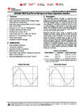
Transcription of LM358/LM2904 低消費電力デュアル汎用オペアンプ
1 LMx58-N 1 8 DSBGA (AN-1112 SNVA009 ) DC 100dB ( ) 1 MHz ( ) 3V 32V 16V (500 A) - 2mV 2 GND VOUT GND 2 4mA 20mA 3 LM158 2 DC LM158 15V lm358 lm2904 TI DSBGA
2 (8 DSBGA) (1) ( )LM158-NTO-CAN (8) (8) (8) (8) (8) (8) (8) (8) (8) (8) (1) (VCO)LM158-N, LM258-N, lm2904 -N, lm358 -NJAJSB93J JANUARY 2000 REVISED MARCH 2022 TI TI English Data Sheet: SNOSBT3 Table of Contents1 ..12 ..13 ..14 Revision Pin Configuration and Absolute Maximum ESD Recommended Operating Thermal Electrical Characteristics: LM158A, LM358A, LM158, Electrical Characteristics: lm358 , Typical Detailed Functional Block Feature Device Functional Application and Application Typical Power Supply Layout Layout Device and Documentation Receiving Notification of Documentation.
3 Electrostatic Discharge Mechanical, Packaging, and Orderable Revision History Changes from Revision I (December 2014) to Revision J (March 2022)Page ..1 Corrected pin 5 (+INB) and pin 7 (OUTB) description information in the Pin Configuration and Functions Deleted Related Links from the Device and Documentation Support from Revision H (March 2013) to Revision I (December 2014)Page ESD ..1 Changes from Revision G (March 2013) to Revision H (March 2013)Page TI.
4 1LM158-N, LM258-N, lm2904 -N, lm358 -NJAJSB93J JANUARY 2000 REVISED MARCH Document FeedbackCopyright 2022 Texas Instruments IncorporatedProduct Folder Links: LM158-N LM258-N lm2904 -N lm358 -N5 Pin Configuration and Functions 5-1. D, P, and NAB Package 8-Pin SOIC, PDIP, and CDIP (Top View) 5-2. LMC Package 8-Pin TO-99 Top View 5-3. YPB Package 8-Pin DSBGA Top View 5-1. Pin FunctionsPINTYPE(1)DESCRIPTIONNAMED/P/LM CYPBOUTA1A1 OOutput, channel A INA2B1 IInverting input, channel A+INA3C1 INon-inverting input, channel AGND / V 4C2 PGround for single-supply configurations. Negative supply for dual-supply configurations.+INB5C3 INon-inverting input, channel B INB6B3 IInverting input, channel BOUTB7A3 OOutput, channel BV+8A2 PPositive supply(1)Signal Types: I = Input, O = Output, I/O = Input or Output, P = , LM258-N, lm2904 -N, lm358 -NJAJSB93J JANUARY 2000 REVISED MARCH 2022 Copyright 2022 Texas Instruments IncorporatedSubmit Document Feedback3 Product Folder Links: LM158-N LM258-N lm2904 -N lm358 -N6 Absolute Maximum RatingsSee (1) (2) (3).
5 LM158, LM258, lm358 , LM158A, LM258A, lm358 ALM2904 UNITMINMAXMINMAXS upply Voltage, V+3226 VDifferential Input Voltage3226 VInput Voltage Dissipation(4) PDIP (P)830830mWTO-99 (LMC)550mWSOIC (D)530530mWDSBGA (YPB)435mWOutput Short-Circuit to GND (One Amplifier)(5)V+ 15 V and TA = 25 CContinuousContinuousInput Current (VIN < )(6)5050mATemperature 55125 CPDIP Package (P): Soldering (10 seconds)260260 CSOIC Package (D)Vapor Phase (60 seconds)215215 CInfrared (15 seconds)220220 CLead TemperaturePDIP (P): (Soldering, 10 seconds)260260 CTO-99 (LMC): (Soldering, 10 seconds)300300 CStorage temperature, Tstg 65150 65150 C(1)Absolute Maximum Ratings indicate limits beyond which damage to the device may occur.
6 Recommended Operating Conditions indicate conditions for which the device is intended to be functional, but specific performance is not ensured. For ensured specifications and the test conditions, see the Electrical Characteristics.(2)Refer to RETS158AX for LM158A military specifications and to RETS158X for LM158 military specifications.(3)If Military/Aerospace specified devices are required, please contact the TI Sales Office/Distributors for availability and specifications.(4)For operating at high temperatures, the lm358 /LM358A, lm2904 must be derated based on a 125 C maximum junction temperature and a thermal resistance of 120 C/W for PDIP, 182 C/W for TO-99, 189 C/W for SOIC package, and 230 C/W for DSBGA, which applies for the device soldered in a printed circuit board, operating in a still air ambient.
7 The LM258/LM258A and LM158/LM158A can be derated based on a +150 C maximum junction temperature. The dissipation is the total of both amplifiers use external resistors, where possible, to allow the amplifier to saturate or to reduce the power which is dissipated in the integrated circuit.(5)Short circuits from the output to V+ can cause excessive heating and eventual destruction. When considering short circuits to ground, the maximum output current is approximately 40 mA independent of the magnitude of V+. At values of supply voltage in excess of +15 V, continuous short-circuits can exceed the power dissipation ratings and cause eventual destruction. Destructive dissipation can result from simultaneous shorts on all amplifiers.
8 (6)This input current will only exist when the voltage at any of the input leads is driven negative. It is due to the collector-base junction of the input PNP transistors becoming forward biased and thereby acting as input diode clamps. In addition to this diode action, there is also lateral NPN parasitic transistor action on the IC chip. This transistor action can cause the output voltages of the op amps to go to the V+voltage level (or to ground for a large overdrive) for the time duration that an input is driven negative. This is not destructive and normal output states will re-establish when the input voltage, which was negative, again returns to a value greater than V (at 25 C). ESD RatingsVALUEUNITV(ESD)Electrostatic dischargeHuman-body model (HBM), per ANSI/ESDA/JEDEC JS-001(1) 250V(1)JEDEC document JEP155 states that 500-V HBM allows safe manufacturing with a standard ESD control , LM258-N, lm2904 -N, lm358 -NJAJSB93J JANUARY 2000 REVISED MARCH Document FeedbackCopyright 2022 Texas Instruments IncorporatedProduct Folder Links: LM158-N LM258-N lm2904 -N Recommended Operating Conditionsover operating free-air temperature range (unless otherwise noted)MINMAXUNITS upply Voltage (V+ - V-):LM158.
9 LM258, LM3583 ( )32 ( 16)VSupply Voltage (V+ - V-):LM29043 ( )26 ( 13)VOperating Temperature: LM158-55125 COperating Temperature: LM258-2585 COperating Temperature: LM358070 COperating Temperature: lm2904 -4085 Thermal InformationTHERMAL METRIC(1)LM158-N, LM258-N, lm358 -NLM158-NLM2904-N, lm358 -NUNITLMCNABYPBDP8 PINSR JAJunction-to-ambient thermal resistance155132230189120 C/W(1)For more information about traditional and new thermal metrics, see the IC Package Thermal Metrics application report, Electrical Characteristics: LM158A, LM358A, LM158, LM258V+ = + V, See(2), unless otherwise statedPARAMETERTEST CONDITIONSLM158 ALM358 ALM158, LM258 UNITMINTYPMAXMINTYPMAXMINTYPMAXI nput Offset VoltageSee(3), TA = 25 C122325mVInput Bias CurrentIIN(+) or IIN( ), TA = 25 C,20504510045150nAVCM = 0 V,(4)Input Offset CurrentIIN(+) IIN( ), VCM = 0V, TA = 25 C210530330nAInput Common-ModeV+ = 30 V,(5)0V+ + + Range( lm2904 , V+ = 26V), TA = 25 CSupply CurrentOver Full Temperature RangeRL = on All Op AmpsV+ = 30V ( lm2904 V+ = 26V)121212mAV+ = Signal Voltage GainV+ = 15 V, TA = 25 C,RL 2 k , (For VO = 1 V to 11 V)
10 501002510050100V/mVCommon-ModeTA = 25 C,708565857085dBRejection RatioVCM = 0 V to V+ VPower SupplyV+ = 5 V to 30 V651006510065100dBRejection Ratio( lm2904 , V+ = 5 V to 26 V), TA = 25 CPower SupplyV+ = 5 V to 30 V651006510065100dBRejection Ratio( lm2904 , V+ = 5 V to 26 V), TA = 25 CAmplifier-to-Amplifier Couplingf = 1 kHz to 20 kHz, TA = 25 C (Input Referred), See(6) 120 120 , LM258-N, lm2904 -N, lm358 -NJAJSB93J JANUARY 2000 REVISED MARCH 2022 Copyright 2022 Texas Instruments IncorporatedSubmit Document Feedback5 Product Folder Links: LM158-N LM258-N lm2904 -N Electrical Characteristics: LM158A, LM358A, LM158, LM258 (continued)V+ = + V, See(2), unless otherwise statedPARAMETERTEST CONDITIONSLM158 ALM358 ALM158, LM258 UNITMINTYPMAXMINTYPMAXMINTYPMAXO utput CurrentSourceVIN + = 1 V,204020402040mAVIN = 0 V,V+ = 15 V,VO = 2 V, TA = 25 CSinkVIN = 1 V, VIN + = 0 V102010201020mAV+ = 15 V, TA = 25 C,VO = 2 VVIN = 1 V,125012501250 AVIN + = 0 VTA = 25 C, VO = 200 mV,V+ = 15 VShort Circuit to GroundTA = 25 C, See(1), V+ = 15 V406040604060mAInput Offset VoltageSee(3)457mVInput Offset Voltage DriftRS = 0 7157207 V/ CInput Offset CurrentIIN(+) IIN( )3075100nAInput Offset Current DriftRS = 0 102001030010pA/ CInput Bias CurrentIIN(+) or IIN( )
