Transcription of LMZ21701 1 A SIMPLE SWITCHER Nano Module …
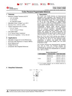
1 Output Current (A)Efficiency (%) = VVOUT = VVOUT = VVOUT = VVOUT = 5 VVINENGNDSSLMZ21701 CINCSSVOUTPGFBVOSCOUTRFBTRFBBVINVOUTP roductFolderOrderNowTechnicalDocumentsTo ols &SoftwareSupport &CommunityReferenceDesignAn IMPORTANTNOTICEat the end of this datasheetaddressesavailability,warranty, changes,use in safety-criticalapplications,intellectual propertymattersand AUGUST2012 REVISEDAUGUST2018 LMZ217011-A Nano ModuleWith 17-V MaximumInput Voltage11 Features1 IntegratedInductor mm mm Package 35-mm SolutionSize(SingleSided) -40 C to 125 C JunctionTemperatureRange AdjustableOutputVoltage IntegratedCompensation AdjustableSoft-StartFunction Startsinto PrebiasedLoads PowerGoodand EnablePins SeamlessTransitionto Power-SaveMode Up to 1000mA OutputCurrent InputVoltageRange3 V to 17 V V to 6 V Efficiencyup to 95 % A ShutdownCurrent 17- A QuiescentCurrent Createa CustomDesignUsingthe LMZ21701 WithWEBENCH PowerDesigner2 Applications V, 5 V, or 12 V InputVoltage SpaceConstrainedApplications LDOR eplacement3 DescriptionThe LMZ21701nanomoduleis an easy-to-usestep-downDC/DCsolutioncapable of drivingup to 1000-mA loadin ,an outputcapacitor,a soft-startcapacitor,andtwo resistorsare requiredfor (1)PARTNUMBERPACKAGEBODYSIZE(NOM)LMZ2170 1 SIP (8) (1)
2 For all availablepackages,see the orderableaddendumatthe end of the VIN= 12 V2 LMZ21701 SNVS853E AUGUST2012 : LMZ21701 SubmitDocumentationFeedbackCopyright 2012 2018,TexasInstrumentsIncorporatedTableof Contents1 Pin Configurationand Applicationand 's and Don'ts ..269 Deviceand Mechanical,Packaging,and RevisionHistoryNOTE:Pagenumbersfor previousrevisionsmay differfrompagenumbersin the (#IMPLIED)to RevisionEPage Addedlinksfor Webenchand top navigatoricon for TI referencedesign; (October2014)to RevisionDPage ChangedfromproductPreviewto Changedto (August2014)to RevisionCPage AddedDeviceInformationand HandlingRatingtables,FeatureDescription, Applicationand ImplementationLayoutDeviceand DocumentationSupportand Mechanical,Packaging,and OrderableInformation, (October2013)to RevisionBPage Updateddatasheetto new TI (August2012)to RevisionAPage (GND)PAD(GND) AUGUST2012 REVISEDAUGUST2018 ProductFolderLinks: LMZ21701 SubmitDocumentationFeedbackCopyright 2012 2018,TexasInstrumentsIncorporated5 Pin Configurationand FunctionsFigure1.
3 LMZ21701in the SIL0008 EPackageSIL Package8-Pin SIPTop ViewPin An externalcapacitorconnectedto this pin sets the can be usedfor trackingand this pin to set the (High= VOUT ready,Low = VOUT belownominalregulation);opendrain(requir espull-upresistor;goeslow impedancewhenEN is low). one terminalof the the powerMOSFET sand and connectionfor the controlloop (High= enabled,Low = disabled).Internalpull downresistorkeepslogiclevellow if pin is left controlcircuitryand solderedto a groundcopperplaneto achieveappropriatepowerdissipationand AUGUST2012 : LMZ21701 SubmitDocumentationFeedbackCopyright 2012 2018,TexasInstrumentsIncorporated(1)Stre ssesbeyondthoselistedunderAbsoluteMaximu mRatingsmay causepermanentdamageto the stressratingsonly,whichdo not implyfunctionaloperationof the deviceat theseor any otherconditionsbeyondthoseindicatedunder RecommendedOperatingConditions.
4 Exposureto absolute-maximum-ratedconditionsfor extendedperiodsmay affectdevicereliability.(2)If Military/Aerospacespecifieddevicesare required,contactthe TexasInstrumentsSalesOffice/Distributors for (unlessotherwisenoted)(1)(2)MINMAXUNITVI N , SS + w/ 20 VmaximumVFB, PG, VOS sink current10mAJunctiontemperature,TJ-MAX 40125 CMaximumlead temperature260 CStoragetemperature,Tstg 65150 C(1)JEDEC documentJEP155statesthat 500-VHBM allowssafe manufacturingwith a standardESDcontrolprocess.(2)JEDEC documentJEP157statesthat 250-VCDM allowssafe manufacturingwith a (ESD)ElectrostaticdischargeHuman-bodymod el(HBM),per ANSI/ESDA/JEDECJS-001(1) 2000 VCharged-devicemodel(CDM),per JEDEC specificationJESD22-C101(2) 500(1)OperatingRatingsindicateconditions for whichthe deviceis intendedto be functional,but do not ,see (unlessotherwisenoted)(1) current01000mAJunctiontemperature,TJ 40125 C(1)For moreinformationabouttraditionaland new thermalmetrics,see theSemiconductorand IC PackageThermalMetricsapplicationreport.
5 (2)Junction-to-ambientthermalresistance( R JA) is basedon 4-layerboardthermalmeasurements,performe dunderthe conditionsandguidelinesset forthin the JEDEC standardsJESD51-1to Avarieswith PCBcopperarea,powerdissipation,and (1) LMZ21701 UNITSIL ( SIP)8 PINSR JAJunction-to-ambientthermalresistance(2 ) C/WR JC(top)Junction-to-case(top) C/WR C/W C/W C/WR JC(bot)Junction-to-case(bottom) AUGUST2012 REVISEDAUGUST2018 ProductFolderLinks: LMZ21701 SubmitDocumentationFeedbackCopyright 2012 2018,TexasInstrumentsIncorporated(1)Min and Max limitsare 100%productiontestedat 25 C. Limitsoverthe operatingtemperaturerangeare ensuredthroughcorrelationusingStatistica lQualityControl(SQC) usedto calculateNational s AverageOutgoingQualityLevel(AOQL).(2)Typ icalnumbersare at 25 C and representthe (1)Limitsapplyoverthe recommendedoperatingjunctiontemperature( TJ) rangeof -40 C to +125 C, Maximumlimitsare specifiedthroughtest, designor mostlikelyparametricnormat TJ= 25 C, and are providedfor followingconditionsapply.
6 VIN= 12 (1)TYP(2)MAX(1)UNITSYSTEMPARAMETERSIQO peratingquiescentcurrentEN = high,IOUT= 0 mA, TJ= -40 C to85 Cdevicenot switching1725 AEN = high,IOUT= 0 mA, TJ= -40 C to125 Cdevicenot switching1728 AISDS hutdowncurrentEN = low, TJ= -40 C to 85 AEN = low, TJ= -40 C to 125 AVINUVLOI nputundervoltagelock out CTSD-HYSTT hermalshutdownhysteresis30 CCONTROLVIH, , = VIN or AVTH_PGPowerGoodthresholdvoltageRising(% VOUT)92%95%98%Falling(% VOUT)87%90%93%VOL_PGPowerGoodoutputlow voltageIPG= -2 V1400nAISSS oftstartPin APOWERSTAGERDS(ON)High-SideMOSFETONR esistanceVIN 6 V82m VIN= 3 V120 Low-SideMOSFETONR esistanceVIN 6 V40m VIN= 3 HDCRI ntegratedpowerinductorDCresistance92m ICL-HSHigh-SideMOSFETC urrentLimitTA= 25 25 (DC)currentlimitVOUT= 5 V, TA= 85 AUGUST2012 : LMZ21701 SubmitDocumentationFeedbackCopyright 2012 2018,TexasInstrumentsIncorporatedElectri calCharacteristics(1)(continued)Limitsap plyoverthe recommendedoperatingjunctiontemperature( TJ) rangeof -40 C to +125 C, Maximumlimitsare specifiedthroughtest, designor mostlikelyparametricnormat TJ= 25 C, and are providedfor followingconditionsapply.
7 VIN= 12 (1)TYP(2)MAX(1) leakagecurrentVFB= V1100nAVOUTL ightload initialvoltageaccuracyPowersavemode,COUT = 22 F, TA=-40 C to 85 C, 1% FB AVOUTLine regulation3 V VIN 17 V, VOUT= V, IOUT= VSYSTEMCHARACTERISTICS Full LoadEfficiencyVOUT= V, IOUT= 1000mA93%LightLoadEfficiencyVOUT= V, IOUT= 1 mA72%Load Current (A)Power Dissipation (W) = 9 VVIN = 12 VVIN = 15 VVIN = 17 VLoad Current (A)Power Dissipation (W) = 5 VVIN = 9 VVIN = 12 VVIN = 15 VVIN = 17 VLoad Current (A)Power Dissipation (W) = VVIN = 5 VVIN = 9 VVIN = 12 VVIN = 15 VVIN = 17 VLoad Current (A)Power Dissipation (W) = VVIN = 5 VVIN = 9 VVIN = 12 VVIN = 15 VVIN = 17 VCopper Area (cm2)Thermal Resistance J-A ( C/W)051015202030405060708090100D0122-LAY ER 70 m (2 oz) Cu4-LAYER 70 m (2 oz) CuLoad Current (A)Power Dissipation (W) = VVIN = 5 VVIN = 9 VVIN = 12 VVIN = 15 VVIN = 17 AUGUST2012 REVISEDAUGUST2018 ProductFolderLinks: LMZ21701 SubmitDocumentationFeedbackCopyright 2012 2018, followingconditionsapply:VIN= 12 V, TA= 25 CFigure2.
8 PackageThermalResistancevs. BoardCopperAreaVOUT= VTA= 85 CFigure3. PowerDissipationVOUT= VTA= 85 CFigure4. PowerDissipationVOUT= VTA= 85 CFigure5. PowerDissipationVOUT= VTA= 85 CFigure6. PowerDissipationVOUT= VTA= 85 CFigure7. PowerDissipationFrequency (MHz)Radiated Emissions (dB V/m)0200400600800100001020304050607080D0 04 Evaluation BoardEN 55022 Class B LimitEN 55022 Class A LimitFrequency (MHz)Conducted Emissions (dB V) EmissionsQuasi Peak LimitAverage LimitInput Voltage (V)Output Voltage (V) = AIOUT = AIOUT = 1 AInput Voltage (V)Output Voltage (V) = AIOUT = AIOUT = 1 A8 LMZ21701 SNVS853E AUGUST2012 : LMZ21701 SubmitDocumentationFeedbackCopyright 2012 2018,TexasInstrumentsIncorporatedTypical Characteristics(continued)Unlessotherwis especifiedthe followingconditionsapply:VIN= 12 V, TA= 25 CVOUT= VTA= 85 CFigure8.
9 DropoutVOUT= VTA= 85 CFigure9. DropoutVIN= 12 VVOUT= VIOUT= 1 AFigure10. RadiatedEMI on EVMVIN= 12 VVOUT= VIOUT= 1 ALf = HCf = FFigure11. ConductedEMI on EVM7 LMZ21701 NanoModuleis an easy-to-usestep-downDC/DCsolutioncapable of drivingup to 1000mA loadin inputcapacitor,an outputcapacitor,a softstartcapacitor,and tworesistorsare requiredfor NanoModulecomesin basedon DCS-Control (DirectControlwithSeamlessTransitioninto PowerSaveMode).Thisarchitecturecombinest he fast transientresponseandstabilityofhystereti ctypeconvertersalongwiththe accurateDC outputregulationof voltagemodeand LMZ21701architectureusespulsewidthmodula tion(PWM)modefor mediumand heavyload requirementsand PowerSaveMode(PSM)at lightloadsfor PWMmodethe switchingfrequencyiscontrolledoverthe valuedependson the outputvoltagesettingand is typicallyreducedat low outputvoltagesto PSMthe switchingfrequencydecreaseslinearlywith architectureof the devicesupportsbothoperationmodes(PWMand PSM)
10 In a singlecircuitbuildingblock,the transitionbetweenthe modesof operationis seamlesswith minimaleffecton the HHIGH SIDE CURRENTLIMITLOW SIDECURRENTLIMITUVLOVREF+-tON TIMERDIRECT CONTROL & COMPENSATIONERROR CLAMPFBVOSPGVOUTVINENSSGND400k SOFTSTART CURRENT AND TRACKING5V LDOTHERMALSHUTDOWNLDOBYPASSHIGH SIDE SWITCHLOW SIDE SWITCHINDUCTOR25pFZERO CURRENTDETECTLOW SIDE DRIVERHIGH SIDE DRIVERWITH INTERNAL BOOTSTRAPCFF+-+ AUGUST2012 REVISEDAUGUST2018 ProductFolderLinks: LMZ21701 SubmitDocumentationFeedbackCopyright 2012 2018, orderto achievea smallsolutionsizethe LMZ21701 NanoModulecomesin an innovativeMicroSiP constructionconsistsof a synchronousbuckconverterIC embeddedinsidean FR-4laminatesubstrate,with a powerinductormountedon top of the Figure12 and Figure13 bottom(landingpads)of the packageresemblea the Mechanicaldrawingsat the end of the datasheetfor detailson the recommendedlandingpatternand BUCK ICFR-4 LAMINATESUBSTRATEBOTTOM COPPER PATTERN10 LMZ21701 SNVS853E AUGUST2012 : LMZ21701 SubmitDocumentationFeedbackCopyright 2012 2018,TexasInstrumentsIncorporatedPackage Construction(continued)Figure12.