Transcription of MAX14808/MAX14809 Octal Three-Level/Quad Five-Level …
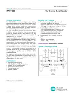
1 EVALUATION KIT AVAILABLE. MAX14808/MAX14809 . Octal Three-Level/Quad Five-Level High-Voltage 2A Digital Pulsers with T/R Switch General Description Benefits and Features The MAX14808/MAX14809 Octal Three-Level/Quad five- S Save Space (Optimized for High-Channel-Count level, high-voltage (HV) pulser devices generate high- Systems/Portable Systems). frequency HV bipolar pulses (up to Q105V) from low- High Density voltage control logic inputs for driving piezoelectric 8 Channels ( three -Level Operation). transducers in ultrasound systems. All eight channels 4 Channels ( Five-Level Operation) in have embedded overvoltage-protection diodes and an One Package integrated active return-to-zero clamp. Both devices have Integrated Low-Power T/R Switches ( max14808 ). embedded independent (floating) power supplies (FPS) DirectDrive Architecture Eliminates External and level shifters that allow signal transmission without High-Voltage Capacitor the need for external HV capacitors.
2 The max14808 also No External Floating Power Supply (FPS). features eight integrated transmit/receive (T/R) switches. Required The max14809 does not have the T/R switch function. S High Performance (Designed to Enhance Image The devices feature two modes of operation: an Octal three -level pulser mode (with integrated active return- Quality). to-zero clamp) or a quad Five-Level pulser mode. In Octal Excellent -43dBc (typ) THD for Second three -level pulser mode, each channel is controlled by Harmonic at 5 MHz two logic inputs (DINN_ /DINP_) and the active return Sync Function Eliminates Effects of FPGA Jitter to zero features half the current driving of the pulser 1A and Improves Performance in Doppler Mode (typ). In quad Five-Level pulser mode, each channel is Low Propagation Delay 18ns (typ). controlled by three logic inputs and the active return to Strong Active Return to Zero zero has the same current driving of the pulser 2A (typ).
3 S Save Power The devices can operate both in clocked and transparent Low Quiescent Power Dissipation ( mode. In clocked mode, data inputs can be synchronized Channel in Octal Mode). with a clean differential or single-ended clock to reduce Programmable Current Capability phase noise associated with FPGA output signals that are Shutdown Mode and Disable Transmit Mode detrimental for Doppler analysis. In transparent mode, the synchronization feature is disabled and output reflects Applications the data input after a 18ns delay. Both devices feature adjustable maximum current ( to 2A) to reduce power Ultrasound Medical Imaging consumption when full current capability is not required. Industrial Flaw Detection The devices feature integrated grass-clipping diodes Piezoelectric Drivers (with low parasitic capacitance) for receive (Rx) and transmit (Tx) isolations. Both devices feature a damping Test Equipment circuit that can be activated as soon as the transmit burst is over.
4 The damping circuit has a typical on-resistance of 500I. It fully discharges the pulser's output internal node Ordering Information and Functional Diagram appear at end before the grass-clipping diodes. of data sheet. The devices are available in a 68-pin (10mm x 10mm). TQFN package with an exposed pad and are specified over the -40NC to +85NC extended temperature range. DirectDrive is a registered trademark of Maxim Integrated Products, Inc. For related parts and recommended products to use with this part, refer to For pricing, delivery, and ordering information, please contact Maxim Direct at 1-888-629-4642, or visit Maxim's website at 19-6438; Rev 2; 1/14. MAX14808/MAX14809 . Octal Three-Level/Quad Five-Level High-Voltage 2A Digital Pulsers with T/R Switch ABSOLUTE MAXIMUM RATINGS. (All voltages referenced to GND.) THP Logic Output Voltage to + VDD Logic Supply Voltage to + VGPA, VGPB Output Voltage VCC Positive Driver Supply Voltage to + [(VPP_ - ), (VEE + )] to (VPP_ + ).
5 VEE Negative Driver Supply Voltage to + VGNA, VGNB Output Voltage VNNA, VNNB High Negative (VNN_ - ) to min[(VCC + ), (VNN_ + )]. Supply Voltage to + Continuous Power Dissipation (TA = +70 C). VPPA, VPPB High Positive TQFN (derate 50mW/NC above +70 C)..4000mW. Supply Voltage to +110V Operating Temperature -40 C to +85 C. OUT_ Output Voltage to VPP_ Maximum Junction +150 C. LVOUT_ Output Voltage Range Storage Temperature -65 C to +150 C. (100mA Maximum Current).. to + Lead Temperature (soldering, 10s)..+300 C. DINN_, DINP_, CC_, SYNC, to + Soldering Temperature (reflow)..+260 C. CLK, CLK, MODE_ Voltage to (VCC + ). Stresses beyond those listed under Absolute Maximum Ratings may cause permanent damage to the device. These are stress ratings only, and functional opera- tion of the device at these or any other conditions beyond those indicated in the operational sections of the specifications is not implied. Exposure to absolute maximum rating conditions for extended periods may affect device reliability.
6 PACKAGE THERMAL CHARACTERISTICS (Note 1). TQFN. Junction-to-Ambient Thermal Resistance (BJA)..20 C/W Junction-to-Case Thermal Resistance (BJC).. C/W. Note 1: Package thermal resistances were obtained using the method described in JEDEC specification JESD51-7, using a four-layer board. For detailed information on package thermal considerations, refer to DC ELECTRICAL CHARACTERISTICS. (VDD = +3V, VCC = +5V, VEE = -5V, VPPA = +100V, VNNA = -100V, VPPB = +100V, VNNB = -100V, 1 F bypass capacitor between VGNA and VNNA, 1FF bypass capacitor between VGNB and VNNB, 1 F bypass capacitor between VGPA and VPPA, 1 F bypass capacitor between VGPB and VPPB, VLDO_EN = 0V, no load, unless otherwise noted. Typical values are at TA = +25 C.) (Note 2). PARAMETER SYMBOL CONDITIONS MIN TYP MAX UNITS. POWER SUPPLIES (VDD, VCC, VEE, VPP_, VNN_). Logic Supply Voltage VDD + +3 + V. Positive Drive Supply Voltage VCC + +5 + V. Negative Drive Supply Voltage VEE -5 V.
7 High-Side Supply Voltage VPP_ 0 +105 V. Low-Side Supply Voltage VNN_ -105 0 V. VGN_ - External Low-Side LDO Voltage LDO_EN = high 5 V. VNN_. VPP_ - External High-Side LDO Voltage LDO_EN = high 5 V. VGP_. External Floating Power-Supply IVGN_ LDO_EN = high (Note 3) 50 mA. Current from VGN_. External Floating Power-Supply IVGP_ LDO_EN = high (Note 3) 85 mA. Current from VGP_. LOGIC INPUTS/OUTPUTS (DINN_, DINP_, MODE_, SYNC, CC_, LDO_EN). Low-Level Input Threshold VIL x VDD V. High-Level Input Threshold VIH x VDD V. Logic Input Capacitance CIN 4 pF. Maxim Integrated 2. MAX14808/MAX14809 . Octal Three-Level/Quad Five-Level High-Voltage 2A Digital Pulsers with T/R Switch DC ELECTRICAL CHARACTERISTICS (continued). (VDD = +3V, VCC = +5V, VEE = -5V, VPPA = +100V, VNNA = -100V, VPPB = +100V, VNNB = -100V, 1 F bypass capacitor between VGNA and VNNA, 1FF bypass capacitor between VGNB and VNNB, 1 F bypass capacitor between VGPA and VPPA, 1 F bypass capacitor between VGPB and VPPB, VLDO_EN = 0V, no load, unless otherwise noted.)
8 Typical values are at TA = +25 C.) (Note 2). PARAMETER SYMBOL CONDITIONS MIN TYP MAX UNITS. Logic Input Leakage IIN VIN = 0V or VDD -1 0 +1 FA. (All Inputs Except LDO_EN). LDO_EN Pulldown Resistance RLDO_EN 7 10 14 kI. THP Low-Level Output Voltage VOL. Pullup resistor to VDD (RPULLUP = 1kI) x VDD V. CLOCK INPUTS (CLK, CLK) DIFFERENTIAL MODE. Differential Clock Input Voltage VCLKD 2 VP-P. Range Common-Mode Voltage VCLKCM VCC/2 V. VCC/2 VCC/2. Common-Mode Voltage Range VCL V. - + RCLK, Differential 7 kI. Input Resistance RCLK Common mode 23 kI. CCLK, Input Capacitance Capacitance to GND (each input) 4 pF. CCLK. CLOCK INPUTS (CLK, CLK) SINGLE-ENDED MODE (VCLK < ). Low-Level Input VIL CLK x VDD V. High-Level Input VIH CLK x VDD V. Single-Ended Mode Selection VIL CLK V. Threshold Low Single-Ended Mode Selection VIH CLK 1 V. Threshold High Input Capacitance (CLK) CCLK 4 pF. Logic Input Leakage (CLK) ICLK VCLK = 0V or VDD -1 0 +1 FA.
9 Pullup Current (CLK) ICLK VCLK = 0V 120 180 FA. SUPPLY CURRENT SHUTDOWN MODE (MODE0 = Low, MODE1 = Low). VDD Supply Current IDD All inputs connected to GND or VDD 3 FA. VCC Supply Current ICC All inputs connected to GND or VDD 22 FA. VEE Supply Current IEE All inputs connected to GND or VDD 13 FA. VPP_ Supply Current IPP_ All inputs connected to GND or VDD 10 FA. VNN_ Supply Current INN_ All inputs connected to GND or VDD 10 FA. SUPPLY CURRENT DISABLE MODE (MODE0 = High, MODE1 = High). Transparent or single- All inputs 3. ended clock mode VDD Supply Current IDDQ connected to FA. GND or VDD Differential clock 110 190. mode, VCLKD = Maxim Integrated 3. MAX14808/MAX14809 . Octal Three-Level/Quad Five-Level High-Voltage 2A Digital Pulsers with T/R Switch DC ELECTRICAL CHARACTERISTICS (continued). ((VDD = +3V, VCC = +5V, VEE = -5V, VPPA = +100V, VNNA = -100V, VPPB = +100V, VNNB = -100V, 1 F bypass capacitor between VGNA and VNNA, 1FF bypass capacitor between VGNB and VNNB, 1 F bypass capacitor between VGPA and VPPA, 1 F bypass capacitor between VGPB and VPPB, VLDO_EN = 0V, no load, unless otherwise noted.))
10 Typical values are at TA = +25 C.) (Note 2). PARAMETER SYMBOL CONDITIONS MIN TYP MAX UNITS. DINN_ = DINP_ = GND VEE Supply Current IEEQ DINN_ = DINP_ = max14808 13 mA. VDD max14809 2. DINN_ = DINP_ = GND VCC Supply Current ICCQ DINN_ = DINP_ = max14808 mA. VDD max14809 VCC Supply Current Increase in DICC Differential clock mode 5 mA. Clocked Mode VNN_ Total Supply Current INNQ_ All inputs connected to GND or VDD 195 305 FA. (Quiescent Mode). VPP_ Total Supply Current IPPQ_ All inputs connected to GND or VDD 220 340 FA. (Quiescent Mode). T/R switch off, damp off (transparent PPDIS1 Total Power Dissipation per mode). mW. Channel (Disable Mode) DINN_ = DINP_ = max14808 17. PPDIS2. VDD max14809 7. SUPPLY CURRENT Octal three -LEVEL MODE, NO LOAD (MODE0 = High, MODE1 = Low). Transparent or single-ended clock 3. VDD Supply Current (Quiescent All inputs connected mode IDD FA. Mode) to GND or VDD Differential clock mode, VCLKD = 110 190.