Transcription of MMBT3906L, SMMBT3906L General Purpose Transistor
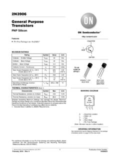
1 Semiconductor Components Industries, LLC, 2013 December, 2013 Rev. 111 Publication Order Number:MMBT3906LT1/DMMBT3906L, SMMBT3906 LGeneral Purpose TransistorPNP SiliconFeatures S Prefix for Automotive and Other Applications Requiring UniqueSite and Control Change Requirements; AEC Q101 Qualified andPPAP Capable These Devices are Pb Free, Halogen Free/BFR Free and are RoHSCompliantMAXIMUM RATINGSR atingSymbolValueUnitCollector Emitter VoltageVCEO 40 VdcCollector Base VoltageVCBO 40 VdcEmitter Base VoltageVEBO Current ContinuousIC 200mAdcCollector Current Peak (Note 3)ICM 800mAdcTHERMAL CHARACTERISTICSC haracteristicSymbolMaxUnitTotal Device Dissipation FR 5 Board(Note 1) @ TA = 25 CDerate above 25 CThermal Resistance, Junction to AmbientRqJA556 C/WTotal Device Dissipation AluminaSubstrate, (Note 2) @ TA = 25 CDerate above 25 CThermal Resistance, Junction to AmbientRqJA417 C/WJunction and Storage TemperatureTJ, Tstg 55 to +150 CStresses exceeding Maximum Ratings may damage the device.
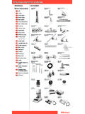
2 MaximumRatings are stress ratings only. Functional operation above the RecommendedOperating Conditions is not implied. Extended exposure to stresses above theRecommended Operating Conditions may affect device FR 5 = Alumina = in. Reference SOA ORDERING INFORMATIONMMBT3906LT1 GSOT 23(Pb Free)3,000 / Tape &Reel For information on tape and reel specifications,including part orientation and tape sizes, pleaserefer to our Tape and Reel Packaging SpecificationsBrochure, BRD8011 23(Pb Free)10,000 / Tape &ReelCOLLECTOR31 BASE2 EMITTERSOT 23 (TO 236)CASE 318 STYLE 6123*Date Code orientation and/or overbar mayvary depending upon manufacturing MGG2A = Specific Device CodeM= Date Code*G= Pb Free Package(Note: Microdot may be in either location)MARKING DIAGRAMSMMBT3906LT1 GSOT 23(Pb Free)3,000 / Tape &ReelSMMBT3906LT3 GSOT 23(Pb Free)10,000 / Tape &ReelMMBT3906L, SMMBT3906 CHARACTERISTICS (TA = 25 C unless otherwise noted)CharacteristicSymbolMinMaxUnitOFF CHARACTERISTICSC ollector Emitter Breakdown Voltage(IC = mAdc, IB = 0)V(BR)CEO 40 VdcCollector Base Breakdown Voltage(IC = 10 mAdc, IE = 0)V(BR)CBO 40 VdcEmitter Base Breakdown Voltage(IE = 10 mAdc, IC = 0)V(BR)EBO VdcBase Cutoff Current(VCE = 30 Vdc, VEB = Vdc)IBL 50nAdcCollector Cutoff Current(VCE = 30 Vdc, VEB = Vdc)ICEX 50nAdcON CHARACTERISTICS (Note 4)DC Current Gain(IC = mAdc, VCE = Vdc)(IC = mAdc, VCE = Vdc)(IC = 10 mAdc, VCE = Vdc)(IC = 50 mAdc, VCE = Vdc)
3 (IC = 100 mAdc, VCE = Vdc)HFE60801006030 300 Collector Emitter Saturation Voltage(IC = 10 mAdc, IB = mAdc)(IC = 50 mAdc, IB = mAdc)VCE(sat) Emitter Saturation Voltage(IC = 10 mAdc, IB = mAdc)(IC = 50 mAdc, IB = mAdc)VBE(sat) SIGNAL CHARACTERISTICSC urrent Gain Bandwidth Product(IC = 10 mAdc, VCE = 20 Vdc, f = 100 MHz)fT250 MHzOutput Capacitance(VCB = Vdc, IE = 0, f = MHz)Cobo Capacitance(VEB = Vdc, IC = 0, f = MHz)Cibo 10pFInput Impedance(IC = mAdc, VCE = 10 Vdc, f = kHz) Feedback Ratio(IC = mAdc, VCE = 10 Vdc, f = kHz) 10 4 Small Signal Current Gain(IC = mAdc, VCE = 10 Vdc, f = kHz)hfe100400 Output Admittance(IC = mAdc, VCE = 10 Vdc, f = kHz) Figure(IC = 100 mAdc, VCE = Vdc, RS = kW, f = kHz)NF CHARACTERISTICSD elay Time(VCC = Vdc, VBE = Vdc,IC = 10 mAdc, IB1 = mAdc)td 35nsRise Timetr 35 Storage Time(VCC = Vdc, IC = 10 mAdc,IB1 = IB2 = mAdc)ts 225nsFall Timetf 754.
4 Pulse Test: Pulse Width v 300 ms, Duty Cycle v , SMMBT3906 1. Delay and Rise TimeEquivalent Test CircuitFigure 2. Storage and Fall TimeEquivalent Test Circuit3 V27510 k1N916CS < 4 pF*3 V27510 kCS < 4 pF*< 1 ns+ V300 nsDUTY CYCLE = 2%< 1 ns+ VDUTY CYCLE = 2%t1010 < t1 < 500 ms* Total shunt capacitance of test jig and connectorsTYPICAL TRANSIENT CHARACTERISTICSF igure 3. CapacitanceREVERSE BIAS (VOLTS) 4. Charge DataIC, COLLECTOR CURRENT (mA) = 40 VIC/IB = 10Q, CHARGE (pC) 10203050 70 100200 CAPACITANCE (pF) 102030 = 25 CTJ = 125 CFigure 5. Turn On TimeIC, COLLECTOR CURRENT (mA)7010020030050050 TIME (ns) 6. Fall TimeIC, COLLECTOR CURRENT (mA) , FALL TIME (ns)fVCC = 40 VIB1 = IB2IC/IB = 20IC/IB = 10IC/IB = 10tr @ VCC = Vtd @ VOB = 0 V40 V15 VMMBT3906L, SMMBT3906 AUDIO SMALL SIGNAL CHARACTERISTICSNOISE FIGURE VARIATIONS(VCE = Vdc, TA = 25 C, Bandwidth = Hz)Figure 7.
5 F, FREQUENCY (kHz) 8. Rg, SOURCE RESISTANCE (k OHMS)0NF, NOISE FIGURE (dB) , NOISE FIGURE (dB)f = kHzIC = mAIC = mAIC = 50 mAIC = 100 mASOURCE RESISTANCE = 200 WIC = mASOURCE RESISTANCE = 200 WIC = mASOURCE RESISTANCE = kIC = 100 mASOURCE RESISTANCE = kIC = 50 mAh PARAMETERS(VCE = 10 Vdc, f = kHz, TA = 25 C)Figure 9. Current GainIC, COLLECTOR CURRENT (mA)7010020030050 Figure 10. Output AdmittanceIC, COLLECTOR CURRENT (mA)h , DC CURRENT GAINh , OUTPUT ADMITTANCE ( mhos)Figure 11. Input ImpedanceIC, COLLECTOR CURRENT (mA)Figure 12. Voltage Feedback RatioIC, COLLECTOR CURRENT (mA) , VOLTAGE FEEDBACK RATIO (X 10 )reh , INPUT IMPEDANCE (k OHMS) , SMMBT3906 STATIC CHARACTERISTICSF igure 13. DC Current GainIC, COLLECTOR CURRENT (mA) = 150 C25 C- 55 ChFE, DC CURRENT GAIN101001000 VCE = 1 VFigure 14.
6 Collector Saturation RegionIB, BASE CURRENT (mA) , COLLECTOR EMITTER VOLTAGE (VOLTS) = mATJ = 25 mA30 mA100 mAMMBT3906L, SMMBT3906 15. Collector Emitter Saturation Voltagevs. Collector CurrentFigure 16. Base Emitter Saturation Voltage CurrentIC, COLLECTOR CURRENT (A)IC, COLLECTOR CURRENT (A) 17. Base Emitter Voltage vs. CollectorCurrentIC, COLLECTOR CURRENT (A) (sat), COLLECTOR EMITTERSATURATION VOLTAGE (V)VBE(sat), BASE EMITTERSATURATION VOLTAGE (V)VBE(on), BASE EMITTER VOLTAGE (V) = 10150 C25 C 55 CIC/IB = 10150 C25 C 55 CVCE = 1 V150 C25 C 55 18. Current Gain Bandwidth CurrentIC, COLLECTOR CURRENT (mA) , CURRENT GAIN BANDWIDTHPRODUCT (MHz)VCE = 2 VTA = 25 CVCE (Vdc) (A)Single Pulse Test@ TA = 25 CThermal Limit100 ms1 s10 ms1 msIC, COLLECTOR CURRENT (mA)- +25 C TO +125 C- 55 C TO +25 C+25 C TO +125 C- 55 C TO +25 CqVC FOR VCE(sat)qVB FOR VBE(sat), TEMPERATURE COEFFICIENTS (mV/ C) VqFigure 19.
7 Temperature CoefficientsFigure 20. Safe Operating AreaMMBT3906L, SMMBT3906 DIMENSIONSSOT 23 (TO 236)CASE 318 08 ISSUE AP mminches SCALE 10 *For additional information on our Pb Free strategy and solderingdetails, please download the ON Semiconductor Soldering andMounting Techniques Reference Manual, FOOTPRINT*STYLE 6:PIN 1. BASE2. EMITTER3. COLLECTORDA1312 NOTES:1. DIMENSIONING AND TOLERANCING PER ANSI , CONTROLLING DIMENSION: MAXIMUM LEAD THICKNESS INCLUDES LEAD FINISHTHICKNESS. MINIMUM LEAD THICKNESS IS THE MINIMUMTHICKNESS OF BASE DIMENSIONS D AND E DO NOT INCLUDE MOLD FLASH,PROTRUSIONS, OR GATE VIEW 100 10q ON Semiconductor and are registered trademarks of Semiconductor Components Industries, LLC (SCILLC). SCILLC reserves the right to make changes without further noticeto any products herein.
8 SCILLC makes no warranty, representation or guarantee regarding the suitability of its products for any particular Purpose , nor does SCILLC assume any liabilityarising out of the application or use of any product or circuit, and specifically disclaims any and all liability, including without limitation special, consequential or incidental damages. Typical parameters which may be provided in SCILLC data sheets and/or specifications can and do vary in different applications and actual performance may vary over time. Alloperating parameters, including Typicals must be validated for each customer application by customer s technical experts. SCILLC does not convey any license under its patent rightsnor the rights of others. SCILLC products are not designed, intended, or authorized for use as components in systems intended for surgical implant into the body, or other applicationsintended to support or sustain life, or for any other application in which the failure of the SCILLC product could create a situation where personal injury or death may occur.
9 ShouldBuyer purchase or use SCILLC products for any such unintended or unauthorized application, Buyer shall indemnify and hold SCILLC and its officers, employees, subsidiaries, affiliates,and distributors harmless against all claims, costs, damages, and expenses, and reasonable attorney fees arising out of, directly or indirectly, any claim of personal injury or deathassociated with such unintended or unauthorized use, even if such claim alleges that SCILLC was negligent regarding the design or manufacture of the part. SCILLC is an EqualOpportunity/Affirmative Action Employer. This literature is subject to all applicable copyright laws and is not for resale in any ORDERING INFORMATIONN. American Technical Support: 800 282 9855 Toll FreeUSA/CanadaEurope, Middle East and Africa Technical Support:Phone: 421 33 790 2910 Japan Customer Focus CenterPhone: 81 3 5817 1050 MMBT3906LT1/DLITERATURE FULFILLMENT:Literature Distribution Center for ON Box 5163, Denver, Colorado 80217 USAP hone: 303 675 2175 or 800 344 3860 Toll Free USA/CanadaFax: 303 675 2176 or 800 344 3867 Toll Free USA/CanadaEmail: Semiconductor Website: Literature: additional information, please contact your localSales Representativ