Transcription of BC856ALT1 - General Purpose Transistors
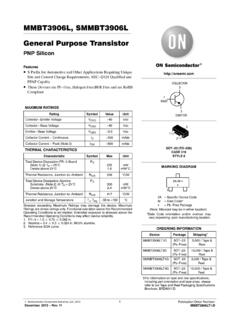
1 Semiconductor Components Industries, LLC, 1994 October, 2016 Rev. 15 Publication Order Number:BC856 ALT1/D1BC856 ALT1G SeriesGeneral PurposeTransistorsPNP SiliconFeatures S and NSV Prefix for Automotive and Other Applications RequiringUnique Site and Control Change Requirements; AEC Q101 Qualified and PPAP Capable These Devices are Pb Free, Halogen Free/BFR Free and are RoHSCompliantMAXIMUM RATINGS (TA = 25 C unless otherwise noted)RatingSymbolValueUnitCollector-Emi tter VoltageBC856, SBC856BC857, SBC857BC858, NSVBC858, BC859 VCEO 65 45 30 VCollector-Base VoltageBC856, SBC856BC857, SBC857BC858, NSVBC858, BC859 VCBO 80 50 30 VEmitter Base VoltageVEBO Current ContinuousIC 100mAdcCollector Current PeakIC 200mAdcTHERMAL CHARACTERISTICSC haracteristicSymbolMaxUnitTotal Device Dissipation FR 5 Board,(Note 1)
2 TA = 25 CDerate above 25 CThermal Resistance,Junction to AmbientRqJA556 C/WTotal Device Dissipation AluminaSubstrate, (Note 2) TA = 25 CDerate above 25 CThermal Resistance,Junction to AmbientRqJA417 C/WJunction and Storage TemperatureTJ, Tstg 55 to +150 CStresses exceeding those listed in the Maximum Ratings table may damage thedevice. If any of these limits are exceeded, device functionality should not beassumed, damage may occur and reliability may be FR 5 = x x Alumina = x x in 23 (TO 236)CASE 318 STYLE 6123 COLLECTOR31 BASE2 EMITTERSee detailed ordering and shipping information in the packagedimensions section on page 6 of this data INFORMATIONMARKING DIAGRAMxx MGGxx= Device Codexx = (Refer to page 6)M= Date Code*G= Pb Free Package(Note.)
3 Microdot may be in either location)*Date Code orientation and/or overbar mayvary depending upon manufacturing CHARACTERISTICS (TA = 25 C unless otherwise noted)CharacteristicSymbolMinTypMaxUnitO FF CHARACTERISTICSC ollector Emitter Breakdown VoltageBC856, SBC856 Series(IC = 10 mA)BC857, SBC857 SeriesBC858, NSBVC858 BC859 SeriesV(BR)CEO 65 45 30 VCollector Emitter Breakdown VoltageBC856 S, SBC856eries(IC = 10 mA, VEB = 0)BC857A, SBC857A, BC857B, SBC857B OnlyBC858, NSVB858, BC859 SeriesV(BR)CES 80 50 30 VCollector Base Breakdown VoltageBC856, SBC856 Series(IC = 10 mA)BC857, SBC857 SeriesBC858, NSVBC858, BC859 SeriesV(BR)CBO 80 50 30 VEmitter Base Breakdown VoltageBC856, SBC856 Series(IE = mA)BC857, SBC857 SeriesBC858, NSVBC858, BC859 SeriesV(BR)EBO VCollector Cutoff Current (VCB = 30 V)Collector Cutoff Current (VCB = 30 V, TA = 150 C)ICBO 15 CHARACTERISTICSDC Current GainBC856A, SBC856A, BC857A, SBC857A, BC858A(IC = 10 mA, VCE = V) BC856B, SBC856B, BC857B, SBC857B,BC858B, NSVBC858 BBC857C, SBC857C BC858C(IC = mA, VCE = V)
4 BC856A, SBC856A, BC857A, SBC857A, BC858 ABC856B, SBC856B, BC857B, SBC857B, BC858B, NSVBC858B, BC859 BBC857C, SBC857C, BC858C, BC859 ChFE 12522042090150270180290520 250475800 Collector Emitter Saturation Voltage(IC = 10 mA, IB = mA)(IC = 100 mA, IB = mA)VCE(sat) Emitter Saturation Voltage(IC = 10 mA, IB = mA)(IC = 100 mA, IB = mA)VBE(sat) VBase Emitter On Voltage(IC = mA, VCE = V)(IC = 10 mA, VCE = V)VBE(on) SIGNAL CHARACTERISTICSC urrent Gain Bandwidth Product(IC = 10 mA, VCE = Vdc, f = 100 MHz)fT100 MHzOutput Capacitance(VCB = 10 V, f = MHz)Cob Figure(IC = mA, VCE = Vdc, RS = kW, f = kHz, BW = 200 Hz)BC856, SBC856, BC857, SBC857, BC858, NSVBC858 SeriesBC859 SeriesNF parametric performance is indicated in the Electrical Characteristics for the listed test conditions, unless otherwise noted.
5 Productperformance may not be indicated by the Electrical Characteristics if operated under different 1. Normalized DC Current GainIC, COLLECTOR CURRENT (mAdc) 2. Saturation and On VoltagesIC, COLLECTOR CURRENT (mAdc) 3. Collector Saturation RegionIB, BASE CURRENT (mA)Figure 4. Base Emitter Temperature CoefficientIC, COLLECTOR CURRENT (mA) , NORMALIZED DC CURRENT GAINV, VOLTAGE (VOLTS)VCE, COLLECTOR-EMITTER VOLTAGE (V)VB, TEMPERATURE COEFFICIENT (mV/ C) = 25 CVBE(sat) @ IC/IB = 10 VCE(sat) @ IC/IB = 10 VBE(on) @ VCE = -10 VVCE = -10 VTA = 25 C-55 C to +125 CIC = -100 mAIC = -20 -10-20-50-100 = -200 mAIC = -50 mAIC =-10 mAFigure 5.
6 CapacitancesVR, REVERSE VOLTAGE (VOLTS)10 Figure 6. Current Gain Bandwidth ProductIC, COLLECTOR CURRENT (mAdc) , CAPACITANCE (pF)f , CURRENT-GAIN - BANDWIDTH PRODUCT (MHz)TTA = 25 -30 = -10 VTA = 25 CTA = 25 7. DC Current GainIC, COLLECTOR CURRENT (mA)Figure 8. On VoltageIC, COLLECTOR CURRENT (mA) = 25 CVBE(sat) @ IC/IB = 10 VCE(sat) @ IC/IB = 10 VBE @ VCE = VFigure 9. Collector Saturation RegionIB, BASE CURRENT (mA)Figure 10. Base Emitter Temperature CoefficientIC, COLLECTOR CURRENT (mA) , COLLECTOR-EMITTER VOLTAGE (VOLTS)VB, TEMPERATURE COEFFICIENT (mV/ C) = 25 CIC =-10 mAhFE, DC CURRENT GAIN (NORMALIZED)V, VOLTAGE (VOLTS)VCE = VTA = 25 mA-20 C to 125 CqVB for 11.
7 CapacitanceVR, REVERSE VOLTAGE (VOLTS)40 Figure 12. Current Gain Bandwidth ProductIC, COLLECTOR CURRENT (mA) = VC, CAPACITANCE (pF)f , CURRENT-GAIN - BANDWIDTH = 25 mA-200 mABC856 ALT1G 13. Thermal Responset, TIME (ms) (t), TRANSIENT (NORMALIZED) k 10 kFigure 14. Active Region Safe Operating AreaVCE, COLLECTOR-EMITTER VOLTAGE (V) , COLLECTOR CURRENT (mA)TA = 25 CD = PULSESINGLE PULSEBONDING WIRE LIMITTHERMAL LIMITSECOND BREAKDOWN LIMIT3 msTJ = 25 CZqJC(t) = r(t) RqJCRqJC = C/W MAXZqJA(t) = r(t) RqJARqJA = 200 C/W MAXD CURVES APPLY FOR POWERPULSE TRAIN SHOWNREAD TIME AT t1TJ(pk) - TC = P(pk) RqJC(t)t1t2P(pk)DUTY CYCLE, D = t1 -65-1001 sBC558, BC559BC557BC556 The safe operating area curves indicate IC VCE limits ofthe transistor that must be observed for reliable load lines for specific circuits must fall below thelimits indicated by the applicable data of Figure 14 is based upon TJ(pk) = 150 C; TC orTA is variable depending upon conditions.
8 Pulse curves arevalid for duty cycles to 10% provided TJ(pk) 150 C. TJ(pk)may be calculated from the data in Figure 13. At high case orambient temperatures, thermal limitations will reduce thepower that can be handled to values less than the limitationsimposed by the secondary INFORMATIOND eviceMarkingPackageShipping BC856 ALT1G3 ASOT 23(Pb Free)3,000 / Tape & ReelSBC856 ALT1G*BC856 ALT3G10,000 / Tape & ReelBC856 BLT1G3 BSOT 23(Pb Free)3,000 / Tape & ReelSBC856 BLT1G*BC856 BLT3G10,000 / Tape & ReelSBC856 BLT3G*BC857 ALT1G3 ESOT 23(Pb Free)3,000 / Tape & ReelSBC857 ALT1G*BC857 BLT1G3 FSOT 23(Pb Free)3,000 / Tape & ReelSBC857 BLT1G*BC857 BLT3G10,000 / Tape & ReelNSVBC857 BLT3G*BC857 CLT1G3 GSOT 23(Pb Free)
9 3,000 / Tape & ReelSBC857 CLT1G*BC857 CLT3G10,000 / Tape & ReelBC858 ALT1G3 JSOT 23(Pb Free)3,000 / Tape & ReelBC858 BLT1G3 KSOT 23(Pb Free)NSVBC858 BLT1G*BC858 BLT3G3 LSOT 23(Pb Free)10,000 / Tape & ReelBC858 CLT1 GSOT 23(Pb Free)3,000 / Tape & ReelBC858 CLT3 GSOT 23(Pb Free)10,000 / Tape & ReelBC859 BLT1G4 BSOT 23(Pb Free)3,000 / Tape & ReelBC859 BLT3 GSOT 23(Pb Free)10,000 / Tape & ReelBC859 CLT1G4 CSOT 23(Pb Free)3,000 / Tape & ReelBC859 CLT3 GSOT 23(Pb Free)10,000 / Tape & Reel For information on tape and reel specifications, including part orientation and tape sizes, please refer to our Tape and Reel PackagingSpecifications Brochure, BRD8011/D.
10 *S and NSV Prefix for Automotive and Other Applications Requiring Unique Site and Control Change Requirements; AEC Q101 Qualifiedand PPAP 23 (TO 236)CASE 318 08 ISSUE ASDATE 30 JAN 2018 SCALE 4:1DA13121 XXXMGGXXX = Specific Device CodeM= Date CodeG= Pb Free Package*This information is generic. Please refer todevice data sheet for actual part Free indicator, G or microdot G ,may or may not be DIAGRAM*NOTES:1. DIMENSIONING AND TOLERANCING PER ASME , CONTROLLING DIMENSION: MAXIMUM LEAD THICKNESS INCLUDES LEAD LEAD THICKNESS IS THE MINIMUM THICKNESS OFTHE BASE DIMENSIONS D AND E DO NOT INCLUDE MOLD FLASH,PROTRUSIONS, OR GATE FOOTPRINTVIEW VIEW 22:PIN 1.
