Transcription of N-Channel Reduced Qg, Fast Switching MOSFET
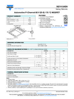
1 vishay SiliconixSi4850 EYDocument Number: 71146S09-1341-Rev. F, Reduced Qg, fast Switching MOSFETFEATURES Halogen-free According to IEC 61249-2-21 Definition TrenchFET Power mosfets 175 C Maximum Junction Temperature Compliant to RoHS Directive 2002/95/ECPRODUCT SUMMARY VDS (V)RDS(on) ( )ID (A) at VGS = 10 V at VGS = V SD SD SD GD 5 6 7 8 Top View 2 3 4 1 Ordering Information: Si4850EY-T1-E3 (Lead (Pb)-free) Si4850EY-T1-GE3 (Lead (Pb)-free and Halogen-free) DGSN- channel MOSFETN otes: a. Surface Mounted on 1" x 1" FR4 board. ABSOLUTE MAXIMUM RATINGS TA = 25 C, unless otherwise notedParameter Symbol 10 sSteady State Unit Drain-Source Voltage VDS60 VGate-Source Voltage VGS 20 Continuous Drain Current (TJ = 175 C)
2 ATA = 25 = 70 Drain Current IDM40 Avalanche CurrentIAS15 Single Pulse Avalanche EnergyEAS11mJMaximum Power DissipationaTA = 25 = 70 Junction and Storage Temperature Range TJ, Tstg- 55 to 175 CTHERMAL RESISTANCE RATINGS Parameter Symbol TypicalMaximumUnit Maximum Junction-to-Ambient at 10 sRthJA3645 C/WSteady State7590 Maximum Junction-to-Foot (Drain)Steady Number: 71146S09-1341-Rev.
3 F, 13-Jul-09 vishay SiliconixSi4850 EYNotes:a. Pulse test; pulse width 300 s, duty cycle 2 %.b. Guaranteed by design, not subject to production testing. Stresses beyond those listed under Absolute Maximum Ratings may cause permanent damage to the device. These are stress ratings only, and functional operationof the device at these or any other conditions beyond those indicated in the operational sections of the specifications is not implied. Exposure to absolute maximumrating conditions for extended periods may affect device CHARACTERISTICS 25 C, unless otherwise notedSPECIFICATIONS TJ = 25 C, unless otherwise notedParameter Symbol Test Conditions StaticDrain-Source Breakdown VoltageVDS VGS = 0 V.
4 ID = 250 A 60 VGate Threshold VoltageVGS(th) VDS = VGS, ID = 250 A 13 Gate-Body LeakageIGSSVDS = 0 V, VGS = 20 V 100 nAZero Gate Voltage Drain CurrentIDSSVDS = 60 V, VGS = 0 V 1 AVDS = 60 V, VGS = 0 V, TJ = 55 C 20On-State Drain CurrentaID(on) VDS 5 V, VGS = 10 V 40 ADrain-Source On-State ResistanceaRDS(on) VGS = 10 V, ID = A VGS = 10 V, ID = A, TJ = 125 = 10 V, ID = A, TJ = 175 C = V, ID = A Transconductanceagfs VDS = 15 V, ID = A 25 SDiode Forward VoltageaVSDIS = A, VGS = 0 V Gate ChargeQg VDS = 30 V, VGS = 10 V, ID = A 1827nCGate-Source ChargeQgs ChargeQgd ResistanceRgVGS = V, f = 5 Tu r n - O n D e l a y T i m etd(on) VDD = 30 V, RL = 30 ID 1 A, VGEN = 10 V, Rg = 6 1020nsRise Timetr1020 Turn-Off Delay Timetd(off)
5 2550 Fall Timetf1224 Source-Drain Reverse Recovery TimetrrIF = A, dI/dt = 100 A/ s5080 Output = 10 V thru 5 V4 V3 VID - Drain Current (A)VDS - Drain-to-Source Voltage (V)Transfer Characteristics0816243240012345- 55 C25 CID - Drain Current (A)VGS - Gate-to-Source Voltage (V)TC = 150 CDocument Number: 71146S09-1341-Rev. F, SiliconixSi4850 EYTYPICAL CHARACTERISTICS 25 C, unless otherwise notedOn-Resistance vs. Drain CurrentGate ChargeSource-Drain Diode Forward = VRDS(on) - On-Resistance ( )ID - Drain Current (A)VGS = 10 V0246810048121620ID = VVDS = 30 VQg - Total Gate Charge (nC)VGS - Gate-to-Source Voltage (V) = 25 CTJ = 175 CIS - Source Current (A)VSD - Source-to-Drain Voltage (V)CapacitanceOn-Resistance vs.
6 Junction TemperatureOn-Resistance vs. Gate-to-Source Voltage02004006008001000120014000 102030405060 CrssCossCissC - Capacitance (pF)VDS - Drain-to-Source Voltage (V) 50 - 250255075100 125 150 175 VGS = 10 VID = ARDS(on) - On-Resistance (Normalized)TJ - Junction Temperature ( C) = AVGS - Gate-to-Source Voltage (V)RDS(on) - On-Resistance ( ) Number: 71146S09-1341-Rev. F, 13-Jul-09 vishay SiliconixSi4850 EYTYPICAL CHARACTERISTICS 25 C, unless otherwise notedVishay Siliconix maintains worldwide manufacturing capability. Products may be manufactured at one of several qualified locations.
7 Reliability data for SiliconTechnology and Package Reliability represent a composite of all qualified locations. For related documents such as package/tape drawings, part marking, andreliability data, see Voltage- 50- 250255075100 125 150 175ID = 250 A VGS(th) Variance (V)TJ - Temperature ( C)Single Pulse (s)1040)W( rewoP100 Normalized Thermal Transient Impedance, PulseDuty Cycle = Wave Pulse Duration (s) evitceffE dezilamroNtneisnarTecnadepmI lamrehT1. Duty Cycle, D = 2. Per Unit Base = R thJA = 75 C/W 3.
8 T JM - TA = PDMZthJA(t)t 1 t 2 t 1 t 2 Notes: 4. Surface Mounted P DM Normalized Thermal Transient Impedance, PulseDuty Cycle = Wave Pulse Duration (s) evitceffE dezilamroNtneisnarTecnadepmI lamrehTVishay SiliconixPackage InformationDocument Number: 8 0 8 : C-06527-Rev. I, 11-Sep-06 DWG: 549843125687 HEh x 45 CAll " mm (Gage Plane)SOIC (NARROW): 8-LEADJEDEC Part Number: MS-012 SApplication Note 826 vishay Siliconix Number: 7260622 Revision: 21-Jan-08 APPLICATION NOTERECOMMENDED MINIMUM PADS FOR ( )Recommended Minimum PadsDimensions in Inches/(mm) ( ) ( ) ( ) ( ) ( ) ( )Return to IndexReturn to IndexLegal Disclaimer Revision: 08-Feb-171 Document Number.
9 91000 Disclaimer ALL PRODUCT, PRODUCT SPECIFICATIONS AND DATA ARE SUBJECT TO CHANGE WITHOUT NOTICE TO IMPROVE RELIABILITY, FUNCTION OR DESIGN OR OTHERWISE. vishay Intertechnology, Inc., its affiliates, agents, and employees, and all persons acting on its or their behalf (collectively, vishay ), disclaim any and all liability for any errors, inaccuracies or incompleteness contained in any datasheet or in any other disclosure relating to any makes no warranty, representation or guarantee regarding the suitability of the products for any particular purpose or the continuing production of any product.
10 To the maximum extent permitted by applicable law, vishay disclaims (i) any and all liability arising out of the application or use of any product, (ii) any and all liability, including without limitation special, consequential or incidental damages, and (iii) any and all implied warranties, including warranties of fitness for particular purpose, non-infringement and merchantability. Statements regarding the suitability of products for certain types of applications are based on vishay s knowledge of typical requirements that are often placed on vishay products in generic applications.
