Transcription of 電力電子元件簡介 - 清華大學電機系-NTHUEE
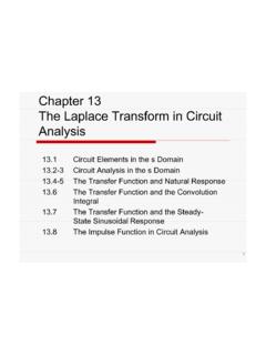
1 Introduction to Power Electronic Devices C. M. Liaw Department of Electrical Engineering National Tsing Hua University Hsinchu, Taiwan, ROC.. ( Power diode) ( SCR). Power diode SCR. AC P. AC. source source Load Load Firing circuit Diode: Uncontrolled turn-on and SCR: Controlled turn-on and turn-off uncontrolled turn-off .. Page 1. ( ). Voltage/current ratings Switching frequency (speed). Switching time On-state resistance (or on-state voltage/current).. (A) (Thyristor) (Silicon Controlled . Rectifier, SCR) : Controlled turn-on, uncontrolled turn-off (B) (Bidirectional Thyristor TRIAC). (C) GTO (Gate Turn-off Thysistor). (D) (Integrated Gate-Commutated Thyristor, IGCT): It is introduced by ABB in 1997. It is a high-voltage, hard-driven, asymmetrical-blocking GTO with unity gain. The gate drive circuit is built-in on the device module. (E) (Power BJT) : Current control device (F) IGBT (Insulated Gate Bipolar Transistor): - Combines the conduction characteristic of BJT and the control characteristic of the MOSFET.
2 (G) MOS (MOS -controlled Thyristor, MCT): - Combines the load characteristic of the thyristor and the control characteristic of the MOSFET. - Low on-state voltage (H) (Power MOSFET) : Voltage control device (I) . Page 2.. (1) Uncontrolled turn-on and off: (diode). (2) Controlled turn-on and uncontrolled turn-off: (SCR). (3) Controlled turn-on and off (Controllable switches): (GTO, IGCT, MCT, BJT, IGBT, MOSFET). (4) Continuous gate signal requirement: (IGCT, BJT, IGBT, MOSFET). (5) Pulse gate signal requirement: (MCT, SCR, TRIAC, GTO). (6) Bipolar voltage-withstanding capability: (SCR). (7) Unipolar voltage-withstanding capability: (GTO, IGCT, MCT, BJT, IGBT, MOSFET). (8) Bidirectional current capability: (TRIAC). (9) Unidirectional current capability: (SCR, GTO, IGCT, MCT, BJT, IGBT, MOSFET, diode). Power Semiconductors Classification of SiC. state-of-the-art Power Semi- conductors Page 3.. ( ). Power Input Power Output Output source source filter Converter filter (to load).
3 (AC, DC). ( / . ( ) Loads: ). Power supplies Switching Feedback Command Control Signal Motor drives Generator ( ).. : : (Cycloconverter). ( ). (Converter): Phase control, integral cycle control (Inverter): VVVF, VVFF. (Chopper): PWM control, FM control Page 4. ?? . (1) . (2) .. (3) . (4) . (5) ( ) . (6) . (7) . (8) . (9) ( ) .. Power diodes: General purpose (for high-power rectification). High speed (for switching application). Schottky (for extra-low voltage rectification). Thyristors Power transistors Page 5. SCR ( ). (Thyristor)- (Silicon Controlled Rectifier, SCR) : Controlled turn-on, uncontrolled turn-off Construction, symbol, equivalent circuit, triggering control, v-i characteristics: A A A. A. P P. N Q1. N N. G. G. P P P i c1 = ib2. G i c2 = ib1. G Q2. N N. K. K K. K. Two-transistor model Page 6. SCR . v AK > V RB (V RWM ) Breakdown i AK. A. i AK 0. P. N. RB. - G FB. P IH iG1 > iG2 > iG3. vAK. N. RB + VRB (VRWM ). VFB (VBO ). K. SCR . : i AK. A. i AK. P. FB.
4 N + IH iG1 > iG2 > iG3. G RB VRB (VRWM ) vAK. P. N. FB - VFB (VBO ). iGK. K. Page 7. Two-transistor model ib i c ib i c (Current is cumulatively amplified). Normally triggered: v AK > 0 i GS > 0. A. Abnormally triggered: High dv/dt High temperature Q1. v AK > V FB. i c1 = i b 2. i c2 = i b1. Q2. G. K.. Turn on: v AK > 0 i GS > 0. Turn off: i AK < I H ( Holding current ).. i AK. V FB V RB . VRB (VRWM ). IH iG1 > iG2 > iG3. vAK. VFB (VBO ). Page 8. Gate SCR . (Shockley diode). on off: v AK V FB ON , i AK < I H OFF. A K. Triac (AC Thyristor). A three-terminal, five layer, bilateral semiconductor device. Bidirectional TRIode AC thyristor. TRIAC. Tab electrically connected to T2. T1. T2. G. Page 9. Triac . TRIAC. Power supply IT48TH. - + - +. T1 T2 G. TRIAC. T2. A three-terminal, five layer, bilateral semiconductor device. P2 N3. T 2 T1 : P2 - N2 - P1 - N1. T 1 T 2 : P1 - N2 - P2 - N3. N2. P1. N1 N4. T1 G. Page 10. TRIAC: SCR . bidirectional current capability . G. T1 ( A ) T2 ( K ) T1 T2.
5 G. v AK > 0 i GK > 0. Turn on: v AK < 0 i GK < 0. Turn off: i AK < I H ( Holding current ). i AK. + iT =. T2 iT 2 - T 1. vT = VRB IH iG 1 > iG 2 > iG 3. vT 2-T1 G vT. T1. VFB 2 -T1. - iG (v AK ). Typical Applications of SCR and TRIAC. n Converter power control (1) Phase control (2) Integral cycle control n SSR (Solid State Relay) or AC Switch Page 11. (Controllable Switches). iT. (1) Forced-commutated SCR Control +. vT. (2) BJT, MOSFET, IGBT, MCT, .. signal - pT =vT iT.. : Switching speed -- : Switching losses . (1) Off : Leakage current vT iT. V ON. (2) On : R ON. , V ON. t p T = v T iT. iT. R ON. V ON Conduction loss . turn-on turn-off (Switching losses). Power BJT. Current-controlled device IB C. B. IC. E. Turn on: I B I C ,sat / b min Page 12. Power BJT. Voltage ratings: (primary breakdown). BV SUS , BV CEO , BV CBO. VCB , max (E is open circuited). VCE , max (B is open circuited). VCE ,max when I C 0. Secondary breakdown: Caused by large di/dt at turn-on instant.
6 Power BJT. b is smaller compared with small-signal BJTs. Hard saturation and quasi-saturation: Quasi-saturation: iC. I B = I C ,sat / b min IB. Hard-saturation: Conduction loss v CE. Switching speed I B > I C , sat / b min Page 13. Power MOSFET. Voltage-controlled device Turn on: v GS > v GS , th i G ,steady - state 0 (very small). D. v GS. v GS G. v GS , th Parasitic C S. Power MOSFET. v GS ,max > v GS > v GS ,th v GS - i D ,sat - , Ron , Pswitching - R DS ,on = k BV DS. 2 .5 ~ 2 . 7. n Light load: Switching loss dominant : iD 1 / Ron v GS P g = Q g vGS f sw vGS2 > vGS1. Q g = total gate charge vGS1. n Heavy load: iD2 > iD1. iD1. Conduction loss dominant : v GS - R DS ,on v DS. Page 14. Cool MOSFET. It is a new revolutionary technology for high voltage power MOSFETs. It implements a compensation structure in the vertical drift region of a MOSFET in order to improve the on-state resistance. R DS ,on , Q g , q JA slightly higher (~ 10%). Pulse current rating is lower.
7 Page 15. Page 16. Page 17. Page 18. Page 19. Power MOSFET Power BJT . Power MOSFET R ON. (Enhancement mode). V ON. {. D v GS > v GS ,th , i G , steady - state 0( very small ).. G Turn on: . switching speed +. {. v GS. - S VON = 0, RON .. : Thermal run away . Power BJT. {. I B > I C,sat / bmin , . C Turn on: . B IC switching speed MOSFET . {. IB E V ON = V CE , sat , R ON.. MOSFET . : Thermal run away . Page 20. IGBT (Insulated-Gate Bipolar Transistor). MOSTFET + BJT. IGBT (Insulated Gate Bipolar Transistor): - Combines the conduction characteristic of BJT. and the control characteristic of the MOSFET. Symbol and equivalent circuit: C(D). C(D) C(D). C(D). G G G. G. E(S) E(S). E(S). E(S). v GS. C(D). G. E(S). Printed circuit .. board Damping filter Page 21. MCT (MOS-controlled Thyristor). MOSTFET + Thyristor Combines the load characteristic of thyristor and the control characteristic of MOSFET. Low on-state voltage A(Anode). Symbol G. K (Cathode). A. Turn on: VGA. p-ch MOSFET M1 D2.}}}}
8 BJT Q2 G. M2 S1. MCT on G. S2. Q1. D1. Turn off: VGA M1 +. n-ch MOSFET M2. BJT Q1 Thyristor Q2 - K. MCT off. Page 22. Triggering Devices ( ).. n (Shockley diode), Four-layer diode n DIAC. n UJT (Uni-junction Transistor). n PUT (Programmable Uni-junction Transistor). n SUS (Silicon Unilateral Switch). n SBS (Silicon Unilateral Switch). n . (Shockley diode). Gate SCR . on off: v AK V FB ON , i AK < I H OFF. A K. Page 23. DIAC ( Gate TRIAC). on off: v AK > 0: v AK V FB ON , i AK < I H OFF. v AK < 0: v AK V RB ON , i AK < I H OFF. i AK.. T1 T2 VRB IH v AK. IH VFB. (Uni-Junction Transistor, UJT). UJT. B2. B2. E rB 2. VD. E. rB1. p n + IE. V EB. - B1. B1. B2. TO-18 package B1. B2 electrically E connected to case Page 24. Emitter Characteristic Curve I E ( mA ). B2. E I E VEB. +. +. VBB. VEB. IE - V P. IV VEB (V ). B1. - VV VP. rB1 D. Peak voltage V p = VD + VB2, B1 = VD + hVB2, B1. rB1 + rB2. D rB1. h= : ( Intrinsic standoff ratio , ). rB1 + rB 2. Application: Relaxation OSC.
9 ( ). V C1. VP. VV t R1 R2 V o1. T R1 C1. + T2 Vo1. E B2. VBB. B1 G T1. - C1. +. +. t V C1 R3 Vo2. - - T R1 C1. Vo 2. t Positive going pulse Page 25. Programmable Unijunction Transistor, PJT). PJT. A A G. G A. P G. Q1. N. n P. N Q2. K. K K. R3 D. V p = VD + VBB = VD + hVBB. R2 + R3. h . R3 D. V p = VD + VBB = VD + hVBB. R2 + R3. R1. R2. T2. Vo3. + Vo1 A. G. Vo2 G T1. VBB. - K. C1 R4. R3. Page 26. SiC (Silicon Carbide) Power Devices Page 27. Introduction to SiC. Silicon Carbide (SiC) is a wide-bandgap semiconductor, which has been intensively studied in the recent years, due to its physical properties , such as high breakdown field, high saturated drift velocity and high thermal conductivity. This characteristics make SiC a very good candidate for the applications in which high temperature, high radiation intensity, high voltage or high power dissipation are involved, such as temperature sensors, nuclear radiation detectors, UV detectors, microwave devices and power devices.
10 Although of the high potential of this material for the use in the electronic industry, the SiC. technology shows some limitations and requires further study in order to obtain electronic devices of the same quality standards as Si technology: the bulk growth of SiC is still very expensive and material quality is still lower than device production requirements;. the epitaxial growth is necessary to obtain device-quality material, but it requires high temperature processes;. selective doping of SiC layers requires the use of ion implantation, since the diffusion coefficients for the doping species are too small for practical applications;. the realization of ohmic contacts on SiC is difficult and requires high temperature processes;. the thermal oxidation of SiC is difficult due to the high temperature needed and the quality of the material obtained is still lower respect to Si oxidation. These limitations underline the need of further study in the SiC field. In particular, the growth of epitaxial layers is a first-step process for the realization of a wide variety of electronic devices.