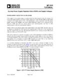
Transcription of Objectives Introduction - The University of Texas …
1 EE/CE 3111 Electronic Circuits Laboratory Spring 2015 Professor Y. Chiu 1 Lab 7: operational Amplifiers Part I Objectives The objective of this lab is to study operational amplifier (op amp) and its applications. We will be simulating and building some basic op amp circuits, including the four most common types, , the inverting, non inverting, differencing, and summing amplifiers. Introduction operational amplifier is one fundamental building block of analog circuits. When used properly in negative feedback configurations, the overall closed loop transfer characteristic can be precisely set by stable passive components such as resistors, capacitors, and diodes, regardless of the potential variation of open loop parameters.
2 Negative feedback amplifier with op amp operating at its core provides key to highly reliable and stable analog functions. In this lab, we will be simulating four basic configurations using the A741 op amp. You can get the A741 part from the library called EVAL. Note that the amplifier has two terminals labeled os1 and os2 besides the regular pins, and you can leave these two pins unconnected. (In case you are curious, these pins are used for offset adjustment for the op amp.) Figure 7 1: Inverting amplifier configuration 1. Inverting amplifier An inverting amplifier is shown in Fig. 7 1. The principal features of this configuration are The amplifier is inverting with the feedback loop closed. The closed loop gain is solely determined by the feedback resistors Rf and Ri assuming that the loop gain defined as the product of the open loop gain of the op amp and the feedback factor of the circuit is very large.
3 The positive input terminal is always grounded in this configuration. As a result, the negative EE/CE 3111 Electronic Circuits Laboratory Spring 2015 Professor Y. Chiu 2 input must follow the potential of the positive one with feedback loop closed due to the large loop gain developed by the op amp. This is often referred to as the virtual ground property of feedback op amps. The closed loop gain of this amplifier is (7 1) Figure 7 2: Non inverting amplifier configuration 2. Non inverting amplifier A non inverting amplifier is shown in Fig. 7 2. The principal features of this configuration are The amplifier is non inverting with the feedback loop closed. The closed loop gain is solely determined by the feedback resistors Rf and Ri assuming that the loop gain of the circuit is very large.
4 The positive input terminal now is connected to the input voltage source. The feedback path, however, is still connected around the output terminal and the negative input terminal. The closed loop gain of this amplifier is 1 (7 2) The input resistance of this configuration is very large. 3. Differencing amplifier A differencing amplifier is shown in Fig. 7 3. The principal features of this configuration are The amplifier can combine two inputs and obtain the difference with the feedback loop closed. The closed loop gain is solely determined by the feedback resistors Rf, Ri, R1 and R2. In this circuit , we set Rf = R1 and Ri = R2. Thus, the output is (7 3) EE/CE 3111 Electronic Circuits Laboratory Spring 2015 Professor Y.
5 Chiu 3 The gains for the positive and negative inputs can be set differently by choosing different R1 and R2 values from above. Figure 7 3: Differencing amplifier configuration Figure 7 4: Summing amplifier configuration 4. Summing amplifier A summing amplifier is shown in Fig. 7 4. The principal features of this configuration are The amplifier is inverting for all inputs with the feedback loop closed. The summing is performed at the negative input terminal in current domain due to the virtual ground property (note that the positive input is grounded). The negative input terminal thus is EE/CE 3111 Electronic Circuits Laboratory Spring 2015 Professor Y. Chiu 4 often referred to as the summing node in such context.
6 The weight for each parallel input is solely determined by the resistor connecting this input to the summing node. The output voltage is a linear combination of all the input voltages. Preparation 1. Perform hand calculation to determine the feedback factor of the op amp for all four circuits in Figs. 1 4. Tabulate your results. 2. Enter the schematics in Fig. 7 1 into PSpice a. Perform bias analysis to find all terminal voltages of the op amp. b. Devise a DC or AC simulation to determine the closed loop gain. 3. Enter the schematics in Fig. 7 2 into PSpice a. Perform bias analysis to find all terminal voltages of the op amp. b. Devise a DC or AC simulation to determine the closed loop gain. 4. Enter the schematics in Fig.
7 7 3 into PSpice a. Perform bias analysis to find all terminal voltages of the op amp. b. Devise a DC or AC simulation to determine the closed loop gain in terms of V3 c. Devise a DC or AC simulation to determine the closed loop gain in terms of V4 5. Determine an expression for the output voltage of the amplifier in Fig. 7 4. 6. Enter the schematics in Fig. 7 4 for two inputs (V3 and V4 in Fig. 7 4) into PSpice a. Perform bias analysis to find all terminal voltages of the op amp. b. Devise a DC or AC simulation to determine the closed loop gain in terms of V3 c. Devise a DC or AC simulation to determine the closed loop gain in terms of V4 Procedure 1. Assemble the four circuits shown in Figs. 1 4 and measure the output voltage and the input terminal voltages of your op amp.
8 Tabulate your measurement results. 2. Vary V3 slightly by 50 100mV and record the change in the output voltage for all four circuits and determine the closed loop gain from V3 to Vout. Tabulate your results. Analysis 1. What is the amplifier input resistance seen by the input source V3 in Figs. 1 4? 2. Re derive the output voltage of (7 3) when Rf = R1 and Ri = R2 do not hold in general. 3. Determine an analytical expression for the closed loop gain seen by V3 in all four circuits in Figs. 1 4 when the op amp exhibits a finite gain A instead of infinity. Your results should be a function of A and some resistor values of the circuit . 4. Can you reliably determine the open loop gain of your op amp in the four amplifier configurations from the measurement results?
9 Why or why not? In case for yes, please tabulate the gains you determined. EE/CE 3111 Electronic Circuits Laboratory Spring 2015 Professor Y. Chiu 5 Lab 7 Report Instructions Besides the general guidelines, report the following for this lab: The lab report should be segmented into 4 parts: o Inverting amplifier o Non-inverting amplifier o Differencing amplifier o Summing amplifier Each part should be comprised of o the circuit design with PSpice Capture and the simulated voltages at each node as well as the closed-loop gain, o the analytical equation for each amplifier and the calculated output voltage and gain, o the experimental voltage readout with a description of the experimental procedure , o a table of all three values for the op-amp terminal voltages.
10 From simulation, theory, and experiment, o a table of all three values for the closed-loop op-amp gain seen by V3: from simulation, theory, and experiment, o and your explanation of the variations between the three values of the last two steps. Answer the questions in the Analysis section.