Transcription of Optocoupler, Phototransistor Output, High Reliability ...
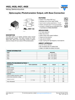
1 Semiconductors Rev. , 31-Aug-151 Document Number: 83740 For technical questions, contact: DOCUMENT IS SUBJECT TO CHANGE WITHOUT NOTICE. THE PRODUCTS DESCRIBED HEREIN AND THIS DOCUMENTARE SUBJECT TO SPECIFIC DISCLAIMERS, SET FORTH AT , Phototransistor Output, High Reliability ,5300 VRMS, 110 C RatedDESCRIPTIONThe 110 C rated SFH617A (DIP) feature a high current transfer ratio, low coupling capacitance and high isolation voltage. These couplers have a GaAs infrared diode emitter, which is optically coupled to a silicon planar Phototransistor detector, and is incorporated in a plastic DIP-4 coupling devices are designed for signal transmission between two electrically separated couplers are end-stackable with mm and clearance distances of > mm are achieved with option Operating temperature from -55 C to +110 C Good CTR linearity depending on forward current Isolation test voltage, 5300 VRMS High collector emitter voltage, VCEO = 70 V Low saturation voltage Fast switching times Low CTR degradation Temperature stable Low coupling capacitance End stackable, " ( mm) spacing High common mode interference immunity Material categorization.
2 For definitions of compliance please see AC adapter SMPS PLC Factory automation Game consolesAGENCY APPROVALSThe safety application model number covering all products in this datasheet is SFH617A. This model number should be used when consulting safety agency documents. UL1577, file no. E52744 cUL tested to CSA bulletin 5A DIN EN 60747-5-5 (VDE 0884-5) available with option 1 BSI IEC 60950; IEC 60065 FIMKO CQCN otes Additional options may be possible, please contact sales office.(1)Also available in tubes; do not add T to INFORMATIONSFH617A- #X0##TPART NUMBERCTR BINPACKAGE OPTION TAPEANDREELAGENCY CERTIFIED/PACKAGECTR (%)UL, BSI, FIMKO, cUL40 to 8063 to 125100 to 200160 to 320 DIP-4 SFH617A-1 SFH617A-2 SFH617A-3 SFH617A-4 DIP-4, 400 mil, option 6 SFH617A-1X006 SFH617A-2X006 SFH617A-3X006 SFH617A-4X006 SMD-4, option 7 SFH617A-1X007T-SFH617A-3X007T-SMD-4, option 9-SFH617A-2X009T--VDE, UL, BSI, FIMKO, cUL40 to 8063 to 125100 to 200160 to 320 DIP-4 SFH617A-1X001 SFH617A-2X001 SFH617A-3X001 SFH617A-4X001 DIP-4, 400 mil, option 6 SFH617A-1X016 SFH617A-2X016 SFH617A-3X016 SFH617A-4X016 SMD-4, option 7-SFH617A-2X017 TSFH617A-3X017T (1)-SMD-4, option 9-SFH617A-2X019T (1) mmOption 7 Option 6 Option 9 DIP-4> 8 mm8 mm Semiconductors Rev.
3 , 31-Aug-152 Document Number: 83740 For technical questions, contact: DOCUMENT IS SUBJECT TO CHANGE WITHOUT NOTICE. THE PRODUCTS DESCRIBED HEREIN AND THIS DOCUMENTARE SUBJECT TO SPECIFIC DISCLAIMERS, SET FORTH AT Stresses in excess of the absolute maximum ratings can cause permanent damage to the device. Functional operation of the device is not implied at these or any other conditions in excess of those given in the operational sections of this document. Exposure to absolute maximum ratings for extended periods of the time can adversely affect Reliability .(1)Refer to reflow profile for soldering conditions for surface mounted devices (SMD). Refer to wave profile for soldering conditions for through hole devices (DIP).Note Minimum and maximum values are testing requirements. Typical values are characteristics of the device and are the result of engineering evaluation.
4 Typical values are for information only and are not part of the testing MAXIMUM RATINGS (Tamb = 25 C, unless otherwise specified)PARAMETERTEST CONDITIONSYMBOLVALUEUNITINPUTR everse voltageVR6 VForward currentIF60mAForward surge currenttp 10 power dissipationat 25 CPdiss70mWOUTPUTC ollector emitter voltageVCEO70 VEmitter collector voltageVECO7 VCollector currentIC50mACollector peak currenttp/T = , tp 10 msICM100mAOuput power dissipationat 25 CPdiss150mWCOUPLERO peration temperatureTamb- 55 to + 110 CStorage temperature rangeTstg- 55 to + 150 CSoldering temperature (1)2 mm from case, 10 sTsld260 CELECTRICAL CHARACTERISTICS (Tamb = 25 C, unless otherwise specified)PARAMETERTEST voltageIF = 60 currentVR = 6 ACapacitanceVR = 0 V, f = 1 MHzCO13pFOUTPUTC ollector emitter capacitanceVCE = 5 V, f = 1 emitter leakage currentVCE = 10 VSFH617A-1 ICEO250nASFH617A-2 ICEO250nASFH617A-3 ICEO5100nASFH617A-4 ICEO5100nACOUPLERC ollector emitter saturation voltageIF = 10 mA, f = 1 Semiconductors Rev.
5 , 31-Aug-153 Document Number: 83740 For technical questions, contact: DOCUMENT IS SUBJECT TO CHANGE WITHOUT NOTICE. THE PRODUCTS DESCRIBED HEREIN AND THIS DOCUMENTARE SUBJECT TO SPECIFIC DISCLAIMERS, SET FORTH AT TRANSFER RATIO (Tamb = 25 C, unless otherwise specified)PARAMETERTEST = 10 mA, VCE = 5 VSFH617A-1 CTR4080%SFH617A-2 CTR63125%SFH617A-3 CTR100200%SFH617A-4 CTR160320%IF = 1 mA, VCE = 5 VSFH617A-1 CTR1330%SFH617A-2 CTR2245%SFH617A-3 CTR3470%SFH617A-4 CTR5690%SWITCHING CHARACTERISTICS (Tamb = 25 C, unless otherwise specified)PARAMETERTEST timeIF = 10 mA, VCC = 5 V, RL = 75 ton3 sRise timeIF = 10 mA, VCC = 5 V, RL = 75 tr2 sTurn-off timeIF = 10 mA, VCC = 5 V, RL = 75 sFall timeIF = 10 mA, VCC = 5 V, RL = 75 tf2 sCut-off frequencyIF = 10 mA, VCC = 5 VfCO100kHzSATURATEDTurn-on timeIF = 20 mASFH617A-1ton3 sIF = 10 sIF = 5 mASFH617A-4ton6 sRise timeIF = 20 mASFH617A-1tr2 sIF = 10 mASFH617A-2tr3 sSFH617A-3tr3 sIF = 5 sTurn-off timeIF = 20 mASFH617A-1toff18 sIF = 10 mASFH617A-2toff23 sSFH617A-3toff23 sIF = 5 mASFH617A-4toff25 sFall timeIF = 20 mASFH617A-1tf11 sIF = 10 mASFH617A-2tf14 sSFH617A-3tf14 sIF = 5 mASFH617A-4tf15 Semiconductors Rev.
6 , 31-Aug-154 Document Number: 83740 For technical questions, contact: DOCUMENT IS SUBJECT TO CHANGE WITHOUT NOTICE. THE PRODUCTS DESCRIBED HEREIN AND THIS DOCUMENTARE SUBJECT TO SPECIFIC DISCLAIMERS, SET FORTH AT 1 - Test Circuit, Non-Saturated OperationFig. 2 - Test Circuit, Saturated OperationFig. 3 - Switching Times Note As per DIN EN 60747-5-5, , this optocoupler is suitable for safe electrical insulation only within the safety ratings. Compliance with the safety ratings shall be ensured by means of protective I Channel II95 10804-3RG = 50 tptp = 50 s T= + 5 V IF050 RLIFO scilloscopeRL= 1 M CL= 20 pFChannel IChannel II95 10843RG= 50 tptp= 50 sT= + 5 VICIF050 1 k IF= 10 mAOscilloscopeRL CL20 pF 1 M tptt0010 %90 %100 %trtdtontstftoffIFICtpPulse durationtdDelay timetrRise timeton(= td + tr) Turn-on timetsStorage timetfFall timetoff(= ts + tf)Turn-off time96 11698 SAFETY AND INSULATION RATINGS PARAMETERTEST CONDITIONSYMBOLVALUEUNITC limatic classificationAccording to IEC 68 part 155/115/21 Pollution degreeAccording to DIN VDE 01092 Comparative tracking index Insulation group IIIaCTI175 Maximum rated withstanding isolation voltageAccording to UL1577, t = 1 min VISO4470 VRMST ested withstanding isolation voltageAccording to UL1577, t = 1 s VISO5300 VRMSM aximum transient isolation voltageAccording to DIN EN 60747-5-5 VIOTM8000 VpeakMaximum repetitive peak isolation voltageAccording to DIN EN 60747-5-5 VIORM890 VpeakIsolation resistanceTamb = 25 C, VIO = 500 VRIO 1012 Tamb = 100 C, VIO = 500 VRIO 1011 Output safety power PSO700mWInput safety current ISI400mAInput safety temperature TS175 CCreepage distanceDIP-4 7mmClearance distanceDIP-4 7mmCreepage distanceDIP-4, 400 mil, option 6 8mmClearance distanceDIP-4.
7 400 mil, option 6 8mmCreepage distanceSMD-4, option 7 and option 9 7mmClearance distanceSMD-4, option 7 and option 9 7mmInsulation thickness DTI Semiconductors Rev. , 31-Aug-155 Document Number: 83740 For technical questions, contact: DOCUMENT IS SUBJECT TO CHANGE WITHOUT NOTICE. THE PRODUCTS DESCRIBED HEREIN AND THIS DOCUMENTARE SUBJECT TO SPECIFIC DISCLAIMERS, SET FORTH AT CHARACTERISTICS (Tamb = 25 C, unless otherwise specified)Fig. 4 - Forward Voltage vs. Forward CurrentFig. 5 - Collector Current vs. Collector Emitter Voltage (NS)Fig. 6 - Collector Current vs. Collector Emitter Voltage (sat)Fig. 7 - Leakage Current vs. Ambient TemperatureFig. 8 - Normalized CTR (NS) vs. Ambient TemperatureFig. 9 - Normalized CTR (sat) vs. Ambient - Forward Current (mA)VF - Forward Voltage (V)Tamb = - 55 = - 40 CTamb = 0 CTamb = 25 CTamb = 50 CTamb = 75 CTamb = 100 CTamb = 110 C020304050607080900178 VCE - Collector Emitter Voltage (NS) (V)IC - Collector Current (mA)1065432IF = 20 mAIF = 15 mAIF = 10 mAIF = 30 mAIF = 5 - Collector Emitter Voltage (sat) (V)IC - Collector Current (mA) = 10 mAIF = 25 mAIF = 5 mAIF = 2 mAIF = 1 000- 60120 Tamb - Ambient Temperature ( C)ICE0 - Leakage Current (nA)10 000 VCE = 40 V- 40100806040200- 20IF = 0 mAVCE = 12 VVCE = 24 60120 Tamb - Ambient Temperature ( C)CTRNorm - Normalized CTR (NS) 40100806040200- 20IF = 5 mAIF = 10 mAIF = 1 mAVCE = 5 60120 Tamb - Ambient Temperature ( C)CTRNorm - Normalized CTR (sat) 40100806040200- 20IF = 5 mAIF = 10 mAIF = 1 mAVCE = Semiconductors Rev.
8 , 31-Aug-156 Document Number: 83740 For technical questions, contact: DOCUMENT IS SUBJECT TO CHANGE WITHOUT NOTICE. THE PRODUCTS DESCRIBED HEREIN AND THIS DOCUMENTARE SUBJECT TO SPECIFIC DISCLAIMERS, SET FORTH AT 10 - Normalized CTR (NS) vs. Forward CurrentFig. 11 - Normalized CTR (sat) vs. Forward CurrentFig. 12 - CTR Frequency vs. Phase AngleFig. 13 - CTR Frequency vs. Collector CurrentFig. 14 - Switching Time vs. Load - Forward Current (mA)CTRNorm - Normalized CTR (NS) = 10 VTamb = - 55 CTamb = - 40 CTamb = 0 CTamb = 25 CTamb = 50 CTamb = 75 CTamb = 100 CTamb = 110 - Forward Current (mA)CTRNorm - Normalized CTR (sat) = - 55 CTamb = - 40 CTamb = 0 CTamb = 25 CTamb = 50 CTamb = 75 CTamb = 100 CTamb = 110 CVCE = V- 140- 120- 100- 80011000f - Frequency (kHz)Phase (deg)- 2010100 VCE = 5 V- 40- - Collector Current (mA)fCTR - CTR Frequency (kHz)100110 VCC = 5 - Load Resistance (k )ton, toff - Switching Time ( s)100110 VCE = 5 V, IF = 10 Semiconductors Rev.
9 , 31-Aug-157 Document Number: 83740 For technical questions, contact: DOCUMENT IS SUBJECT TO CHANGE WITHOUT NOTICE. THE PRODUCTS DESCRIBED HEREIN AND THIS DOCUMENTARE SUBJECT TO SPECIFIC DISCLAIMERS, SET FORTH AT DIMENISONS in millimetersPACKAGE MARKING Notes VDE logo is only marked on option 1 parts. Option information is not marked on the part. Tape and reel suffix (T) is not part of the package 1 to + YWW Semiconductors Rev. , 31-Aug-158 Document Number: 83740 For technical questions, contact: DOCUMENT IS SUBJECT TO CHANGE WITHOUT NOTICE. THE PRODUCTS DESCRIBED HEREIN AND THIS DOCUMENTARE SUBJECT TO SPECIFIC DISCLAIMERS, SET FORTH AT PROFILESFig. 15 - Wave soldering Double Wave Profile According to J-STD-020 for DIP-8 DevicesFig. 16 - Lead (Pb)-free Reflow Solder Profile According to J-STD-020 for SMD-8 DevicesHANDLING AND STORAGE CONDITIONSESD level: HBM class 2 Floor life: unlimitedConditions: Tamb < 30 C, RH < 85 %Moisture sensitivity level 1, according to J-STD-0202 K/ssecondwavefirst wavewaveca.
10 5 K/s5 sfull line: typicaldotted line:process limitsTime (s)Temperature ( C)30025020015010050005010015020025094 8626 Lead temperature235 C to 260 C100 C to 130 Cca. 200 K/sforced coolingca. 2 K/s050100150200250300050100150200250300 Time (s)Temperature ( C)240 C245 Cmax. 260 Cmax. 120 smax. 100 s217 Cmax. 30 smax. ramp up 3 C/smax. ramp down 6 C/s19841255 CLegal Disclaimer Revision: 01-Jan-20221 Document Number: 91000 Disclaimer ALL PRODUCT, PRODUCT SPECIFICATIONS AND DATA ARE SUBJECT TO CHANGE WITHOUT NOTICE TO IMPROVE Reliability , FUNCTION OR DESIGN OR OTHERWISE. Vishay Intertechnology, Inc., its affiliates, agents, and employees, and all persons acting on its or their behalf (collectively, Vishay ), disclaim any and all liability for any errors, inaccuracies or incompleteness contained in any datasheet or in any other disclosure relating to any makes no warranty, representation or guarantee regarding the suitability of the products for any particular purpose or the continuing production of any product.