Transcription of PD - 95810 IRFP1405 - Infineon Technologies
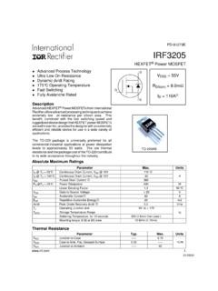
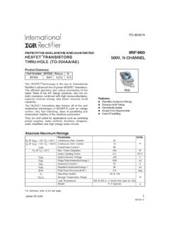
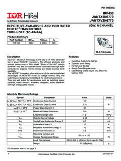
1 HEXFET Power MOSFETVDSS = 55 VRDS(on) = ID = MOSFETPD - 95810 Specifically designed for Automotive applications, this HEXFET Power MOSFET utilizes the latest processing techniques toachieve extremely low on-resistance per silicon area. Additionalfeatures of this design are a 175 C junction operating tempera-ture, fast switching speed and improved repetitive avalancherating . These features combine to make this design an extremelyefficient and reliable device for use in Automotive applications anda wide variety of other Advanced Process Technology Ultra Low On-Resistance 175 C Operating Temperature Fast Switching Repetitive Avalanche Allowed up to TjmaxFeaturesHEXFET is a registered trademark of International Rectifier.*2 2 2 2 2 t2 22WH gIRFP1405TO-247AC hqAbsolute Maximum RatingsParameterUnitsID @ TC = 25 CContinuous Drain Current, VGS @ 10V (Silicon Limited)ID @ TC = 100 CContinuous Drain Current, VGS @ 10V AID @ TC = 25 CContinuous Drain Current, VGS @ 10V (Package Limited)IDMP ulsed Drain Current cPD @TC = 25 CPower Dissipation WLinear Derating Factor W/ CVGSGate-to-Source VoltageVEAS (Thermally limited) Single Pulse Avalanche EnergydmJEAS (Tested ) Single Pulse Avalanche Energy Tested Value hIARA valanche Current cAEARR epetitive Avalanche Energy gmJTJ Operating Junction andTSTGS torage Temperature Range CSoldering Temperature, for 10 secondsMounting Torque, 6-32 or M3 screwThermal JC Junction-to-Case * cs Case-to-Sink, Flat, Greased Surface C/WR JA Junction-to-Ambient * 401060530 See , 12b, 15, to + 175300 ( from case )10 lbfyin ( )s p Characteristics @ TJ = 25 C (unless otherwise specified)ParameterMin.
2 Typ. Max. UnitsV(BR)DSSD rain-to-Source Breakdown Voltage55 V V(BR)DSS/ TJ Breakdown Voltage Temp. Coefficient V/ CRDS(on)Static Drain-to-Source On-Resistance VGS(th)Gate Threshold Transconductance77 SIDSSD rain-to-Source Leakage Current 20 A 250 IGSSGate-to-Source Forward Leakage 200nAGate-to-Source Reverse Leakage -200 QgTotal Gate Charge 120180 QgsGate-to-Source Charge 30 nCQgdGate-to-Drain ("Miller") Charge 53 td(on)Turn-On Delay Time 12 trRise Time 160 td(off)Turn-Off Delay Time 140 nstfFall Time 150 LDInternal Drain Inductance Between lead, nH6mm ( )LSInternal Source Inductance 13 from packageand center of die contactCissInput Capacitance 5600 CossOutput Capacitance 1310 CrssReverse Transfer Capacitance 350 pFCossOutput Capacitance 6550 CossOutput Capacitance 920 Coss Output Capacitance 1750 Source-Drain Ratings and Characteristics ParameterMin.
3 Typ. Max. UnitsISContinuous Source Current 95(Body Diode)AISMP ulsed Source Current 640(Body Diode) cVSDD iode Forward Voltage Recovery Time 70110nsQrrReverse Recovery Charge 170260nCtonForward Turn-On TimeIntrinsic turn-on time is negligible (turn-on is dominated by LS+LD)VGS = 0V, VDS = , = = 0V, VDS = 44V, = = 0V, VDS = 0V to 44V fVGS = 10V eVDD = 28 VID = 95 ARG = TJ = 25 C, IS = 95A, VGS = 0V eTJ = 25 C, IF = 95A, VDD = 28 Vdi/dt = 100A/ s eConditionsVGS = 0V, ID = 250 AReference to 25 C, ID = 1mA VGS = 10V, ID = 95A eVDS = VGS, ID = 250 AVDS = 55V, VGS = 0 VVDS = 55V, VGS = 0V, TJ = 125 CMOSFET symbolshowing theintegral reversep-n junction = 25V, ID = 95 AID = 95 AVDS = 44 VConditionsVGS = 10V eVGS = 0 VVDS = 25V = = 20 VVGS = -20V 2 Repetitive rating; pulse width limited by max. junction temperature. (See fig. 11). 2 Limited by TJmax, starting TJ = 25 C, L = RG = 25 , IAS = 95A, VGS =10V. Part not recommended for use above this value.
4 Pulse width ; duty cycle 2%.x X Coss eff. is a fixed capacitance that gives the same charging time as Coss while VDS is rising from 0 to 80% VDSS . 2 Limited by TJmax , see , 12b, 15, 16 for typical repetitive avalanche performance. 2 This value determined from sample failure population. 100% tested to this value in p 2. Typical Output CharacteristicsFig 1. Typical Output CharacteristicsFig 3. Typical Transfer CharacteristicsFig 4. Typical Forward TransconductanceVs. Drain , Drain-to-Source Voltage (V)101001000ID, Drain-to-Source Current (A) 60 s PULSE WIDTHTj = 175 , Gate-to-Source Voltage (V)101001000ID, Drain-to-Source Current ( )VDS = 25V 60 s PULSE WIDTHTJ = 25 CTJ = 175 , Drain-to-Source Voltage (V)1101001000ID, Drain-to-Source Current (A) 60 s PULSE WIDTHTj = 25 20406080100ID, Drain-to-Source Current (A)020406080100120140 Gfs, Forward Transconductance (S)TJ = 25 CTJ = 175 CVDS = 10V380 s PULSE WIDTHs p 8.
5 Maximum Safe Operating AreaFig 6. Typical Gate Charge VoltageFig 5. Typical Capacitance VoltageFig 7. Typical Source-Drain DiodeForward Voltage110100 VDS, Drain-to-Source Voltage (V)0200040006000800010000C, Capacitance (pF)CossCrssCissVGS = 0V, f = 1 MHZCiss = Cgs + Cgd, Cds SHORTEDCrss = Cgd Coss = Cds + Cgd04080120160200 QG Total Gate Charge (nC)048121620 VGS, Gate-to-Source Voltage (V)VDS= 44 VVDS= 28 VID= 95 AFOR TEST CIRCUITSEE FIGURE , Source-toDrain Voltage (V) , Reverse Drain Current (A)TJ = 25 CTJ = 175 CVGS = 0V1101001000 VDS , Drain-toSource Voltage (V) , Drain-to-Source Current (A)Tc = 25 CTj = 175 CSingle Pulse1msec10msecOPERATION IN THIS AREA LIMITED BY RDS(on)100 secDCs p 11. Maximum Effective Transient Thermal Impedance, Junction-to-CaseFig 9. Maximum Drain Current TemperatureFig 10. Normalized On-ResistanceVs. Temperature255075100125150175 TC , Case Temperature ( C)050100150200ID , Drain Current (A)LIMITED BY PACKAGE-60-40-20020406080100120140160180 TJ , Junction Temperature ( C) (on) , Drain-to-Source On Resistance (Normalized)ID = 95 AVGS = , Rectangular Pulse Duration (sec) Response ( Z thJC ) = PULSE( THERMAL RESPONSE )Notes:1.
6 Duty Factor D = t1/t22. Peak Tj = P dm x Zthjc + TcRi ( C/W) i (sec) J J 1 1 2 2R1R1R2R2 CCii/RiCi= i/Ris p Fig 13b. Gate Charge Test CircuitFig 13a. Basic Gate Charge WaveformFig 12c. Maximum Avalanche EnergyVs. Drain CurrentFig 12b. Unclamped Inductive WaveformsFig 12a. Unclamped Inductive Test CircuittpV(BR)DSSIASFig 14. Threshold Voltage Vs. +-VDDDRIVERA15V20 VVGS255075100125150175 Starting TJ, Junction Temperature ( C)0500100015002000 EAS, Single Pulse Avalanche Energy (mJ) IDTOP 16A 20 ABOTTOM 95A-75-50-250255075100125150175TJ , Temperature ( C ) (th) Gate threshold Voltage (V)ID = 250 A1 KVCCDUT0Ls p 15. Typical Avalanche Current 16. Maximum Avalanche EnergyVs. TemperatureNotes on Repetitive Avalanche Curves , Figures 15, 16:(For further info, see AN-1005 at )1. Avalanche failures assumption: Purely a thermal phenomenon and failure occurs at a temperature far in excess of Tjmax.
7 This is validated for every part Safe operation in Avalanche is allowed as long asTjmax is not Equation below based on circuit and waveforms shown in Figures 12a, PD (ave) = Average power dissipation per single avalanche BV = Rated breakdown voltage ( factor accounts for voltage increase during avalanche).6. Iav = Allowable avalanche T = Allowable rise in junction temperature, not to exceed Tjmax (assumed as 25 C in Figure 15, 16). tav = Average time in avalanche. D = Duty cycle in avalanche = tav f ZthJC(D, tav) = Transient thermal resistance, see figure 11)PD (ave) = 1/2 ( BV Iav) =2hT/ ZthJCIav = 2hT/ [ BV Zth]EAS (AR) = PD (ave) (sec)110100100010000 Avalanche Current (A) Cycle = Single avalanche Current vs avalanche pulsewidth, tav assuming Tj = 25 C due to avalanche losses. Note: In no case should Tj be allowed to exceed TJ , Junction Temperature ( C)0100200300400500600 EAR , Avalanche Energy (mJ)TOP Single Pulse BOTTOM 1% Duty CycleID = 95As p 17.
8 2h 2 2 G 2 2g 2for N-ChannelHEXFET 2 Power MOSFETsg 2v 2g 2v 2 2s 22 q 2 22 v 2v 2s 222222g 2 Recoverydv/dtRipple 5%Body Diode Forward DropRe-AppliedVoltageReverseRecoveryCurr entBody Diode ForwardCurrentVGS=10 VVDDISDD river Gate VDSW aveformInductor CurentD = P. W .PeriodB2 q 2a2S 2 2v " 2v $ 2h $ B+-+++--- q hh G 2 2 2 q h 2 2 ! 2 2hF F F s h2 2 2h 2p 24h4 hF F F2E2h 2 2 hF F VDS90%10%VGStd(on)trtd(off)tf h 2 (2 1 ) h 2p 2 % h q qhF F FIH +- hhFig 18a. Switching Time Test CircuitFig 18b. Switching Time Waveformss p and specifications subject to change without notice. This product has been designed and qualified for Automotive [Q101] Standards can be found on IR s Web packages are not recommended for Surface Mount Application. yEPRUeg2 2y yEPRUeg2 2w 2s Dimensions are shown in millimetersLOT CODEWW = WE E KYY = YE ARNotes : T his part marking information applies to devices produced before 02/26/2001 or forE XAMP L E : T H I S I S AN I R F P E 30 WIT H AS S E MB L Y L OT CODE 3A1 QASSEMBLYLOGORECTIFIERINTERNAT IONAL3A1 QIRF PE30 PART NUMBER(YYWW)DAT E CODE9302par ts manuf actur ed i n GB.
9 Notes : T his part marking information applies to devices produced after 02/26/2001 EXAMPLE:AS S E MB L ED ON WW 35, 2000L OT CODE 5657 WIT H AS S E MB L Y T HIS IS AN IR FPE30 IN T HE ASSEMBLY LINE "H" 035 HLOGOINT ER NAT IONALRECTIFIERIRFPE30 LOT CODEAS S E MB L Y56 57 PART NUMBERDAT E CODEYE AR 0 = 2000WE E K 3 5 LINE HIR WORLD HEADQUARTERS: 233 Kansas St., El Segundo, California 90245, USA Tel: (310) 252-7105 TAC Fax: (310) 252-7903 Visit us at for sales contact '5* 1 Note: For the most current drawings please refer to the IR website at.