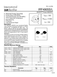
Transcription of Power MOSFET - Vishay
1 IRFP9140, SiHFP9140. Vishay Siliconix Power MOSFET . FEATURES. PRODUCT SUMMARY. Dynamic dV/dt Rating VDS (V) - 100 Available Repetitive Avalanche Rated RDS(on) ( ) VGS = - 10 V P-Channel RoHS*. COMPLIANT. Qg (Max.) (nC) 61. Isolated Central Mounting Hole Qgs (nC) 14. 175 C Operating Temperature Qgd (nC) 29 Fast Switching Configuration Single Ease of Paralleling S Compliant to RoHS Directive 2002/95/EC. TO-247AC. DESCRIPTION. Third generation Power mosfets from Vishay provide the G. designer with the best combination of fast switching, ruggedized device design, low on-resistance and cost-effectiveness. S. The TO-247AC package is preferred for D commercial-industrial applications where higher Power G D levels preclude the use of TO-220AB devices. The P-Channel MOSFET TO-247AC is similar but superior to the earlier TO-218.
2 Package because of its isolated mouting hole. It also provides greater creepage distance between pins to meet the requirements of most safety specifications. ORDERING INFORMATION. Package TO-247AC. IRFP9140 PbF. Lead (Pb)-free SiHFP9140-E3. IRFP9140. SnPb SiHFP9140. ABSOLUTE MAXIMUM RATINGS (TC = 25 C, unless otherwise noted). PARAMETER SYMBOL LIMIT UNIT. Drain-Source Voltage VDS - 100. V. Gate-Source Voltage VGS 20. TC = 25 C - 21. Continuous Drain Current VGS at - 10 V ID. TC = 100 C - 15 A. Pulsed Drain Currenta IDM - 84. Linear Derating Factor W/ C. Single Pulse Avalanche Energyb EAS 960 mJ. Repetitive Avalanche Currenta IAR - 21 A. Repetitive Avalanche Energya EAR 18 mJ. Maximum Power Dissipation TC = 25 C PD 180 W. Peak Diode Recovery dV/dtc dV/dt - V/ns Operating Junction and Storage Temperature Range TJ, Tstg - 55 to + 175.
3 C. Soldering Recommendations (Peak Temperature) for 10 s 300d 10 lbf in Mounting Torque 6-32 or M3 screw N m Notes a. Repetitive rating; pulse width limited by maximum junction temperature (see fig. 11). b. VDD = - 25 V, starting TJ = 25 C, L = mH, Rg = 25 , IAS = - 21 A (see fig. 12). c. ISD - 21 A, dI/dt 200 A/ s, VDD VDS, TJ 175 C. d. mm from case. * Pb containing terminations are not RoHS compliant, exemptions may apply Document Number: 91238 S11-0444-Rev. B, 14-Mar-11 1. This datasheet is subject to change without notice. THE PRODUCT DESCRIBED HEREIN AND THIS DATASHEET ARE SUBJECT TO SPECIFIC DISCLAIMERS, SET FORTH AT IRFP9140, SiHFP9140. Vishay Siliconix THERMAL RESISTANCE RATINGS. PARAMETER SYMBOL TYP. MAX. UNIT. Maximum Junction-to-Ambient RthJA - 40. Case-to-Sink, Flat, Greased Surface RthCS - C/W. Maximum Junction-to-Case (Drain) RthJC - SPECIFICATIONS (TJ = 25 C, unless otherwise noted).
4 PARAMETER SYMBOL TEST CONDITIONS MIN. TYP. MAX. UNIT. Static Drain-Source Breakdown Voltage VDS VGS = 0 V, ID = - 250 A - 100 - - V. VDS Temperature Coefficient VDS/TJ Reference to 25 C, ID = - 1 mA - - - V/ C. Gate-Source Threshold Voltage VGS(th) VDS = VGS, ID = - 250 A - - - V. Gate-Source Leakage IGSS VGS = 20 V - - 100 nA. VDS = - 100 V, VGS = 0 V - - - 100. Zero Gate Voltage Drain Current IDSS A. VDS = - 80 V, VGS = 0 V, TJ = 150 C - - - 500. Drain-Source On-State Resistance RDS(on) VGS = - 10 V ID = - 13 Ab - - . Forward Transconductance gfs VDS = - 50 V, ID = - 13 Ab - - S. Dynamic Input Capacitance Ciss - 1400 - VGS = 0 V, Output Capacitance Coss VDS = - 25 V, - 590 - pF. f = MHz, see fig. 5. Reverse Transfer Capacitance Crss - 140 - Total Gate Charge Qg - - 61. ID = - 19 A, VDS = - 80 V, Gate-Source Charge Qgs VGS = - 10 V - - 14 nC.
5 See fig. 6 and 13b Gate-Drain Charge Qgd - - 29. Turn-On Delay Time td(on) - 16 - Rise Time tr - 73 - VDD = - 50 V, ID = - 19 A, ns Turn-Off Delay Time td(off) Rg = , RD = , see fig. 10b - 34 - Fall Time tf - 57 - Between lead, D. Internal Drain Inductance LD - - 6 mm ( ") from package and center of G. nH. Internal Source Inductance LS die contact - 13 - S. Drain-Source Body Diode Characteristics Continuous Source-Drain Diode Current IS MOSFET symbol D - - - 21. showing the integral reverse A. G. Pulsed Diode Forward Currenta ISM p - n junction diode S. - - - 84. Body Diode Voltage VSD TJ = 25 C, IS = - 21 A, VGS = 0 Vb - - - V. Body Diode Reverse Recovery Time trr - 130 260 ns TJ = 25 C, IF = - 19 A, dI/dt = 100 A/ sb Body Diode Reverse Recovery Charge Qrr - C. Forward Turn-On Time ton Intrinsic turn-on time is negligible (turn-on is dominated by LS and LD).
6 Notes a. Repetitive rating; pulse width limited by maximum junction temperature (see fig. 11). b. Pulse width 300 s; duty cycle 2 %. Document Number: 91238. 2 S11-0444-Rev. B, 14-Mar-11. This datasheet is subject to change without notice. THE PRODUCT DESCRIBED HEREIN AND THIS DATASHEET ARE SUBJECT TO SPECIFIC DISCLAIMERS, SET FORTH AT IRFP9140, SiHFP9140. Vishay Siliconix TYPICAL CHARACTERISTICS (25 C, unless otherwise noted). Fig. 1 - Typical Output Characteristics, TC = 25 C Fig. 3 - Typical Transfer Characteristics Fig. 2 - Typical Output Characteristics, TC = 175 C Fig. 4 - Normalized On-Resistance vs. Temperature Document Number: 91238 S11-0444-Rev. B, 14-Mar-11 3. This datasheet is subject to change without notice. THE PRODUCT DESCRIBED HEREIN AND THIS DATASHEET ARE SUBJECT TO SPECIFIC DISCLAIMERS, SET FORTH AT IRFP9140, SiHFP9140.
7 Vishay Siliconix Fig. 5 - Typical Capacitance vs. Drain-to-Source Voltage Fig. 7 - Typical Source-Drain Diode Forward Voltage Fig. 6 - Typical Gate Charge vs. Gate-to-Source Voltage Fig. 8 - Maximum Safe Operating Area Document Number: 91238. 4 S11-0444-Rev. B, 14-Mar-11. This datasheet is subject to change without notice. THE PRODUCT DESCRIBED HEREIN AND THIS DATASHEET ARE SUBJECT TO SPECIFIC DISCLAIMERS, SET FORTH AT IRFP9140, SiHFP9140. Vishay Siliconix RD. VDS. VGS. RG - +VDD. - 10 V. Pulse width 1 s Duty factor %. Fig. 10a - Switching Time Test Circuit td(on) tr td(off) tf VGS. 10 %. 90 %. VDS. Fig. 9 - Maximum Drain Current vs. Case Temperature Fig. 10b - Switching Time Waveforms Fig. 11 - Maximum Effective Transient Thermal Impedance, Junction-to-Case Document Number: 91238 S11-0444-Rev. B, 14-Mar-11 5. This datasheet is subject to change without notice.
8 THE PRODUCT DESCRIBED HEREIN AND THIS DATASHEET ARE SUBJECT TO SPECIFIC DISCLAIMERS, SET FORTH AT IRFP9140, SiHFP9140. Vishay Siliconix L IAS. VDS. Vary tp to obtain required IAS. VDS. RG - + V DD. IAS VDD. - 10 V tp tp . VDS. Fig. 12a - Unclamped Inductive Test Circuit Fig. 12b - Unclamped Inductive Waveforms Fig. 12c - Maximum Avalanche Energy vs. Drain Current Current regulator Same type as QG 50 k . - 10 V 12 V F. F. QGS QGD - + VDS. VG. VGS. - 3 mA. Charge IG ID. Current sampling resistors Fig. 13a - Basic Gate Charge Waveform Fig. 13b - Gate Charge Test Circuit Document Number: 91238. 6 S11-0444-Rev. B, 14-Mar-11. This datasheet is subject to change without notice. THE PRODUCT DESCRIBED HEREIN AND THIS DATASHEET ARE SUBJECT TO SPECIFIC DISCLAIMERS, SET FORTH AT IRFP9140, SiHFP9140. Vishay Siliconix Peak Diode Recovery dV/dt Test Circuit +.
9 Circuit layout considerations Low stray inductance Ground plane Low leakage inductance current transformer - +. - - +. Rg dV/dt controlled by Rg +. ISD controlled by duty factor D VDD. - device under test - Note Compliment N-Channel of for driver Driver gate drive Period D=. Period VGS = - 10 Va lSD waveform Reverse recovery Body diode forward current current dI/dt VDS waveform Diode recovery dV/dt VDD. Re-applied voltage Body diode forward drop Inductor current ISD. Ripple 5 %. Note a. VGS = - 5 V for logic level and - 3 V drive devices Fig. 14 - For P-Channel Vishay Siliconix maintains worldwide manufacturing capability. Products may be manufactured at one of several qualified locations. Reliability data for Silicon Technology and Package Reliability represent a composite of all qualified locations. For related documents such as package/tape drawings, part marking, and reliability data, see Document Number: 91238 S11-0444-Rev.
10 B, 14-Mar-11 7. This datasheet is subject to change without notice. THE PRODUCT DESCRIBED HEREIN AND THIS DATASHEET ARE SUBJECT TO SPECIFIC DISCLAIMERS, SET FORTH AT Package Information Vishay Siliconix TO-247AC (High Voltage). A A. 4. E 7 P (Datum B). B. E/2 S A2 k M DBM. 3 R/2 P1. A. D2. Q. 4 4. 2xR. D D1. (2). 1 2 3 D 4. Thermal pad 5 L1. C L 4. E1. See view B A. M D B M. 2 x b2 C View A - A. 2x e 3xb b4 A1. M C A M. (b1, b3, b5). Planting Base metal Lead Assignments 1. Gate D DE E. 2. Drain 3. Source (c) c1. C C. 4. Drain (b, b2, b4). (4). Section C - C, D - D, E - E. View B. MILLIMETERS INCHES MILLIMETERS INCHES. DIM. MIN. MAX. MIN. MAX. DIM. MIN. MAX. MIN. MAX. A D2 A1 E A2 E1 - - b e BSC BSC. b1 k b2 L b3 L1 b4 N BSC BSC. b5 P c P1 - - c1 Q D R D1 - - S BSC BSC. ECN: X13-0103-Rev. D, 01-Jul-13. DWG: 5971. Notes 1.