Transcription of RADIATION HARDENED LOGIC LEVEL POWER …
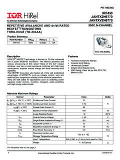
1 Features 5V CMOS and TTL Compatible Fast Switching Single Event Effect (SEE) HARDENED Low Total Gate Charge Simple Drive Requirements Ease of Paralleling Hermetically Sealed Ceramic Package Surface Mount Light Weight ESD Rating: Class 1C per MIL-STD-750, Method 1020 Absolute Maximum Ratings Pre-Irradiation Parameter Units ID @ VGS = , TC = 25 C Continuous Drain Current -22* A ID @ VGS = , TC = 100 C Continuous Drain Current IDM Pulsed Drain Current -88 PD @TC = 25 C Maximum POWER Dissipation 57 W Linear Derating Factor W/ C VGS Gate-to-Source Voltage 10 V EAS Single Pulse Avalanche Energy 79 mJ IAR Avalanche Current -22 A EAR Repetitive Avalanche Energy mJ dv/dt Peak Diode Recovery dv/dt V/ns
2 TJ Operating Junction and -55 to + 150 TSTG Storage Temperature Range Pckg. Mounting Surface Temp. 300 (for 5s) Weight (Typical) g C 2N7624U3 IRHLNJ797034 1 2016-11-14 Product Summary Part Number RADIATION LEVEL RDS(on) ID IRHLNJ797034 100 kRads(Si) -22A* IRHLNJ793034 300 kRads(Si) -22A* RADIATION HARDENED LOGIC LEVEL POWER MOSFET SURFACE MOUNT ( ) * Current is limited by package For Footnotes refer to the page 2. PD-97302D Description R 7 60V, P-CHANNEL TECHNOLOGY IR HiRel R7 LOGIC LEVEL POWER MOSFETs provide simple solution to interfacing CMOS and TTL control circuits to POWER devices in space and other RADIATION environments. The threshold voltage remains within acceptable operating limits over the full operating temperature and post RADIATION .
3 This is achieved while maintaining single event gate rupture and single event burnout immunity. The device is ideal when used to interface directly with most LOGIC gates, linear IC s, micro-controllers, and other device types that operate from a source. It may also be used to increase the output current of a PWM, voltage comparator or an operational amplifier where the LOGIC LEVEL drive signal is available. 2 2016-11-14 IRHLNJ797034, 2N7624U3 Pre-Irradiation Electrical Characteristics @ Tj = 25 C (Unless Otherwise Specified) Parameter Min. Typ. Max. Units Test Conditions BVDSS Drain-to-Source Breakdown Voltage -60 V VGS = 0V, ID = -250 A BVDSS/ TJ Breakdown Voltage Temp.
4 Coefficient V/ C Reference to 25 C, ID = RDS(on) Static Drain-to-Source On-State VGS = , ID = Resistance VGS(th) Gate Threshold Voltage V VGS(th)/ TJ Gate Threshold Voltage Coefficient mV/ C Gfs Forward Transconductance 16 S VDS = -10V, ID = IDSS Zero Gate Voltage Drain Current A VDS = -48V, VGS = 0V -15 VDS = -48V,VGS = 0V,TJ =125 C IGSS Gate-to-Source Leakage Forward -100 nA VGS = -10V Gate-to-Source Leakage Reverse 100 VGS = 10V QG Total Gate Charge 36 nC ID = -22A QGS Gate-to-Source Charge 10 VDS = -30V QGD Gate-to-Drain ( Miller ) Charge 18 VGS = td(on) Turn-On Delay Time 32 ns VDD = -30V tr Rise Time 250 ID = -22A td(off) Turn-Off Delay Time 100 RG = tf Fall Time 102 VGS = Ls +LD Total Inductance nH Measured from the center of drain pad to center of source pad Ciss Input Capacitance 2261 pF VGS = 0V Coss Output Capacitance 583 VDS = -25V Crss Reverse Transfer Capacitance 91 = RG Gate Resistance 20 = ,open drain VDS = VGS, ID = -250 A Source-Drain Diode Ratings and Characteristics Parameter Min.
5 Typ. Max. Units Test Conditions IS Continuous Source Current (Body Diode) -22* ISM Pulsed Source Current (Body Diode) -88 VSD Diode Forward Voltage V TJ = 25 C,IS = -22A, VGS = 0V trr Reverse Recovery Time 110 ns TJ = 25 C,IF = -22A, Qrr Reverse Recovery Charge 132 nC VDD -50V, di/dt = -100A/ s ton Forward Turn-On Time Intrinsic turn-on time is negligible (turn-on is dominated by LS+LD) A Footnotes: Repetitive Rating; Pulse width limited by maximum junction temperature. VDD = -25V, starting TJ = 25 C, L = , Peak IL = -22A, VGS = -10V ISD -22A, di/dt -350A/ s, VDD -60V, TJ 150 C Pulse width 300 s; Duty Cycle 2% Total Dose Irradiation with VGS Bias. -10 volt VGS applied and VDS = 0 during irradiation per MIL-STD-750, Method 1019, condition A.
6 Total Dose Irradiation with VDS Bias. -48 volt VDS applied and VGS = 0 during irradiation per MlL-STD-750, Method 1019, condition A. Thermal Resistance Parameter Min. Typ. Max. Units R JC Junction-to-Case C/W * Current is limited by package 3 2016-11-14 IRHLNJ797034, 2N7624U3 Pre-Irradiation Table1. Electrical Characteristics @ Tj = 25 C, Post Total Dose Irradiation Parameter Up to 300 kRads (Si) 1 Units Test Conditions Min. Max.
7 BVDSS Drain-to-Source Breakdown Voltage -60 V VGS = 0V, ID = -250 A VGS(th) Gate Threshold Voltage V VDS = VGS, ID = -250 A IGSS Gate-to-Source Leakage Forward -100 nA VGS = -10V IGSS Gate-to-Source Leakage Reverse 100 nA VGS = 10V IDSS Zero Gate Voltage Drain Current A VDS = -48V, VGS = 0V RDS(on) Static Drain-to-Source On-State Resistance (TO-3) VGS = , ID = RDS(on) Static Drain-to-Source On-State Resistance ( ) VGS = , ID = VSD Diode Forward Voltage V VGS = 0V, ID = -22A Table 2. Typical Single Event Effect Safe Operating Area LET (MeV/(mg/cm2)) Energy (MeV) Range ( m) VDS (V) @VGS=0V @VGS=2V @VGS= 4V @VGS= 7V 38 5% 300 38 -60 -60 -60 -40 62 5% 355 33 -60 -60 -60 85 5% 380 29 -60 -60 -60 @VGS= 6V -60 @VGS= 5V -60 -60 IR HiRel RADIATION HARDENED MOSFETs have been characterized in heavy ion environment for Single Event Effects (SEE).
8 Single Event Effects characterization is illustrated in Fig. a and Table 2. Fig a. Typical Single Event Effect, Safe Operating Area For Footnotes, refer to the page 2. IR HiRel RADIATION HARDENED MOSFETs are tested to verify their RADIATION hardness capability. The hardness assurance program at IR Hirel is comprised of two RADIATION environments. Every manufacturing lot is tested for total ionizing dose (per notes 5 and 6) using the TO-3 package. Both pre- and post-irradiation performance are tested and specified using the same drive circuitry and test conditions in order to provide a direct comparison. RADIATION Characteristics 1 Part numbers IRHLNJ797034 and IRHLNJ793034 -70-60-50-40-30-20-10001234567 Bias VDS (V)Bias VGS (V)LET=38 5%LET=62 5%LET=85 5%4 2016-11-14 IRHLNJ797034, 2N7624U3 Pre-Irradiation Fig 2.
9 Typical Output Characteristics Fig 3. Typical Transfer Characteristics Fig 1. Typical Output Characteristics Fig 4. Normalized On-Resistance Vs. Temperature , Drain-to-Source Voltage (V)110100-ID, Drain-to-Source Current (A)20 s PULSE WIDTH Tj = 25 C VGSTOP -10V , Drain-to-Source Voltage (V)110100-ID, Drain-to-Source Current (A)20 s PULSE WIDTH Tj = 150 C VGSTOP -10V , Gate-to-Source Voltage (V)110100-ID, Drain-to-Source Current (A)VDS = -25V60 s PULSE WIDTHTJ = 150 CTJ = 25 C-60-40-20020406080100120140160TJ , Junction Temperature ( C) (on) , Drain-to-Source On Resistance (Normalized)
10 VGS = = -22A24681012-VGS, Gate -to -Source Voltage (V)020406080100120140160 RDS(on), Drain-to -Source On Resistance (m )ID = -22 ATJ = 25 CTJ = 150 CFig 5. Typical On-Resistance Vs Gate Voltage 01020304050607080-ID, Drain Current (A)30405060708090100110120130140 RDS(on), Drain-to -Source On Resistance (m )TJ = 25 CTJ = 150 CVgs = Fig 6. Typical On-Resistance Vs Drain Current 5 2016-11-14 IRHLNJ797034, 2N7624U3 Pre-Irradiation -60-40-20020406080100120140160TJ , Temperature ( C ) (th) Gate threshold Voltage (V)ID = -50 AID = -250 AID = = -150mAFig 8. Typical Threshold Voltage Vs Temperature -60-40-20020406080100120140160TJ , Temperature ( C )5560657075-V(BR)DSS, Drain-to-Source Breakdown Voltage (V)ID = 12. Maximum Drain Current Vs. Case Temperature 110100-VDS, Drain-to-Source Voltage (V)04008001200160020002400280032003600C, Capacitance (pF)VGS = 0V, f = 1 MHzCiss = Cgs + Cgd, Cds SHORTEDCrss = Cgd Coss = Cds + CgdCossCrssCissFig 7.